The rise of synthetic 2D polymers: hot charge carriers in the TEM
An international research team has demonstrated that highly mobile 'hot carriers' in a two-dimensional conjugated polymer, Cu₃BHT, can achieve ultrahigh mobility. This breakthrough could accelerate the development of organic-based hot carrier devices for applications like high-speed transistors and efficient photovoltaics.
Hot carriers are high-energy electrons and holes that exist out of thermal equilibrium with the crystal lattice. Their unique properties have driven innovation in fields such as photovoltaics, transistors, photodetectors, photo-catalysis, and bolometers. [1], [2] Recent computational and experimental studies have outlined a general three-stage process for hot carriers: generation, thermalization, and relaxation. [3], [4], [5]
However, the study of hot carriers in organic compounds has significantly lagged behind the understanding of them in inorganic or hybrid materials. This knowledge gap is primarily due to the extremely fast energy relaxation process in conventional organic materials, a limitation caused by dynamic disorder, strong Coulomb interactions between electron-hole pairs, and intense charge-vibrational coupling. [6], [7] [3], [8]
The recent emergence of synthetic two-dimensional (2D) organic crystals, particularly 2D conjugated coordination polymers (2D c-CPs), presents a promising new avenue. These materials display attractive opto-electronic properties stemming from tunable intralayer d-π conjugation and interlayer electronic coupling. [9] Advances in synthesis now allow for precise control over stoichiometry, structure, layer orientation, and morphology, leading to a variety of structures with diverse properties. [10] A key property is their high electrical conductivity, which can reach up to 103 S cm−1. [11]
For hot carrier applications, 2D c-CPs provide an opportunity to engineer electronic and phononic properties at the molecular level. This allows for the creation of high-mobility charge transport channels while simultaneously slowing down the cooling processes of hot carriers. [12] Researchers utilized a combination of time-resolved terahertz spectroscopy (TRTS), transient absorption spectroscopy (TAS), and transient absorption microscopy (TAM) to observe the spatiotemporal evolution of non-equilibrium photoexcitation. This approach was used to track the charge transport properties dependent on excess kinetic energy in a model 2D c-CP system, Cu₃BHT (where BHT is benzenehexathiol; Fig. 1a).
These combined experiments offer a comprehensive view of transport phenomena across temporal, spatial, and frequency domains. The results indicate that photoexcitation above the band gap initiates a transport cascade in highly crystalline Cu₃BHT films. In this non-equilibrium state, hot carriers dominate, demonstrating an exceptionally high charge mobility of approximately 2,000 cm² V⁻¹ s⁻¹ and traveling up to ~300 nm across grain boundaries.
The cooling of these highly mobile hot carriers is relatively slow, occurring over timescales up to ~750 fs. This is attributed to the material's low optical phonon energy and small electron-hole reduced effective mass, making it comparable to state-of-the-art lead-halide perovskites known for their suitability in hot carrier applications. [13] Once the carriers cool and enter a quasi-equilibrium state, these band-edge carriers show band-like Drude-type free carrier transport, with an impressive charge mobility of ~400 cm² V⁻¹ s⁻¹ and an intrinsic diffusion length exceeding 1 μm.
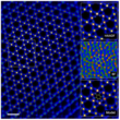
The Cu₃BHT films were synthesized via an optimized liquid-liquid interfacial method [11] and were analyzed using aberration-corrected high-resolution transmission electron microscopy (HRTEM), as shown in Fig. 1b (left). The HRTEM images reveal a highly ordered lattice with atomic resolution (~1.2 Å) and a lattice spacing of ~0.73 nm.
Further analysis with high-angle annular dark-field scanning transmission electron microscopy (Fig. 2) shows a high-symmetry, non-distorted Kagome lattice formed by copper atoms. In this structure, each BHT unit is connected to six neighboring BHT units through shared Cu atoms, and each Cu atom coordinates with four S atoms, creating a dense hexagonal d–π conjugated plane.
Based on AC-HRTEM and GIWAXS analyses, the researchers proposed a triclinic lattice structure with a slipped-AA-stacking geometry. The unit-cell parameters were determined to be a = b = 8.675 Å, c = 3.489 Å, α = β = 99.94°, and γ = 60.12°. The simulated AC-HRTEM image (Fig. 1b, right) and GIWAXS diffraction signals based on this model showed good agreement with experimental observations.
X-ray photoelectron spectroscopy results pointed to a fractional oxidation state of Cu and a square-planar coordination geometry. This is attributed to an intramolecular pseudo-redox mechanism between Cu⁺/Cu²⁺ and the BHT ligands. [14]
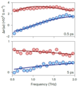
To investigate the microscopic charge transport properties, the team performed TRTS measurements, a contact-free method. In these measurements, an ultrashort pump pulse (~50 fs) with tunable photon energy injects hot carriers into the sample. A subsequent time-delayed, single-cycle terahertz (THz) pulse (~1 ps) passes through the sample, driving the photogenerated carriers over short distances and providing insight into their intracrystal charge transport properties. [15]
The non-resonant excitation led to a sub-picosecond increase in photoconductivity, indicating the quasi-instantaneous generation of mobile carriers. This positive THz photoconductivity confirms the intrinsic semiconducting nature of the Cu₃BHT films. [12] The photoconductivity, Δσ(t), is the product of photogenerated carrier density (n), elementary charge (e), and electron-hole sum mobility (μ), expressed as Δσ(t) = neμ. A fast-decay component observed in the signal could be explained by two possible scenarios.
The first scenario suggests that hot carriers rapidly lose their excess kinetic energy and populate band-edge states within the instrument's time resolution (under ~50 fs). In this case, the fast decay would reflect a reduction in band-edge carrier density due to rapid charge localization or trapping, meaning 'n' decays quickly. [16] The second scenario proposes that hot carriers have much higher mobility than band-edge carriers, and their energy relaxation occurs on a longer timescale (over ~50 fs). Here, the fast decay would signify a decrease in charge mobility ('μ') as the non-equilibrium system relaxes. [17]
As illustrated in Fig. 3, the linear dependence of Δσoffset on the absorbed photon density, Nabs, excludes the defect trapping scenario, which would show a super-linear dependence. [16] This linearity demonstrates that the band-edge carrier density increases linearly with Nabs without reaching absorption saturation or non-radiative Auger relaxation. It also indicates that the mobility μ of the band-edge carriers remains constant, with negligible carrier-carrier interactions in the investigated Nabs range.
The reduced energy dissipation rates in Cu₃BHT are favored by its low optical phonon energy and small electron-hole reduced effective mass. [12] This leads to a relatively long hot carrier lifetime, superior to the sub-100 fs lifetimes typical in conventional organic compounds [6], [7] and comparable to the 200 fs to several picoseconds lifetimes seen in inorganic and hybrid perovskite materials. [13]
Figure 4a displays a pseudo-color 2D image of the transient absorption (TA) spectra of Cu₃BHT at various pump-probe delay times under 1.77 eV photoexcitation. These spectra show a broad photo-induced absorption signal between 2.4–3.0 eV, which exhibits a noticeable blue-shift of about 60 meV within the first few picoseconds (Fig. 4a).
The researchers observed that the temporal evolution of this photo-induced absorption band mirrors the Δσ dynamics, suggesting the spectral blue-shift is linked to hot carrier cooling. [5], [18] This conclusion is supported by the calculated electronic band structure and density of states, which show that transitions from the Cu d-band to the valence band edge can account for the observed photo-induced absorption signal (Fig. 4b).
To confirm this, a global fitting analysis of the TA spectra was performed, identifying two distinct spectral components at 2.69 eV and 2.79 eV (Fig. 5a). As shown in Figure 5b, the peak energy shift, which signifies hot carrier relaxation, evolves in remarkable tandem with the photoconductivity decay. This finding substantiates the blue-shift as a spectroscopic marker for the hot carrier cooling process.
Ressource: Fu, S., Huang, X., Gao, G. et al. Unveiling high-mobility hot carriers in a two-dimensional conjugated coordination polymer. Nature Materials 24, 1457–1464 DOI: 10.1038/s41563-025-02246-2
- Paul, K. K., Kim, J.-H. & Lee, Y. H. (2021). Hot carrier photovoltaics in van der Waals heterostructures. Nat. Rev. Phys. 3, 178–192. [Quelle]
- Liu, C. et al. (2024). A hot-emitter transistor based on stimulated emission of heated carriers. Nature 632, 782–787. [Quelle]
- Jailaubekov, A. E. et al. (2013) Hot charge-transfer excitons set the time limit for charge separation at donor/acceptor interfaces in organic photovoltaics. Nat. Mater. 12, 66–73. [Quelle]
- Fu, J. et al. (2017). Hot carrier cooling mechanisms in halide perovskites. Nat. Commun. 8, 1300. [Quelle]
- Price, M. B. et al. (2015). Hot-carrier cooling and photo-induced refractive index changes in organic–inorganic lead halide perovskites. Nat. Commun. 6, 8420. [Quelle]
- Banerji, N., Cowan, S., Vauthey, E. & Heeger, A. J. (2011). Ultrafast relaxation of the poly(3-hexylthiophene) emission spectrum. J. Phys. Chem. C 115, 9726–9739. [Quelle]
- Engel, E., Koschorreck, M., Leo, K. & Hoffmann, M. (2005). Ultrafast relaxation in quasi-one-dimensional organic molecular crystals. Phys. Rev. Lett. 95, 157403. [Quelle]
- Haldar, R. et al. (2021). Interplay of structural dynamics and electronic effects in an engineered assembly of pentacene in a metal–organic framework. Chem. Sci. 12, 4477–4483. [Quelle]
- Dou, J.-H. et al. (2021). Atomically precise single-crystal structures of electrically conducting 2D metal–organic frameworks. Nat. Mater. 20, 222–228. [Quelle]
- Wang, M., Dong, R. & Feng, X. (2021). Two-dimensional conjugated metal–organic frameworks (2D c-MOFs): chemistry and function for MOFtronics. Chem. Soc. Rev. 50, 2764–2793. [Quelle]
- Huang, X. et al. (2015). A two-dimensional π–d conjugated coordination polymer with extremely high electrical conductivity and ambipolar transport behavior. Nat. Commun. 6, 7408. [Quelle]
- Huang, X. et al. (2023). Semiconducting conjugated coordination polymer with high charge mobility enabled by '4 + 2' phenyl ligands. J. Am. Chem. Soc. 145, 2430–2438. [Quelle]
- Lin, W., Canton, S. E., Zheng, K. & Pullerits, T. (2024). Carrier cooling in lead halide perovskites: a perspective on hot carrier solar cells. ACS Energy Lett. 9, 298–307. [Quelle]
- Toyoda, R. et al. (2022). Heterometallic benzenehexathiolato coordination nanosheets: periodic structure improves crystallinity and electrical conductivity. Adv. Mater. 34, 2106204. [Quelle]
- Ulbricht, R., Hendry, E., Shan, J., Heinz, T. F. & Bonn, M. (2011). Carrier dynamics in semiconductors studied with time-resolved terahertz spectroscopy. Rev. Mod. Phys. 83, 543–586. [Quelle]
- Uhd Jepsen, P. et al. (2001). Ultrafast carrier trapping in microcrystalline silicon observed in optical pump–terahertz probe measurements. Appl. Phys. Lett. 79, 1291–1293. [Quelle]
- Zhang, H. et al. (2021). Highly mobile hot holes in Cs2AgBiBr6 double perovskite. Sci. Adv. 7, eabj9066. [Quelle]
- Lim, J. W. M. et al. (2020). Hot carriers in halide perovskites: how hot truly? J. Phys. Chem. Lett. 11, 2743–2750. [Quelle]


