Outline Research
Recently, scientists rediscovered the advantages of using low energies in transmission electron microscopy for imaging low-Z number material. In the nearest future, the analysis of soft/hard matter device structures of classical crystalline as well as carbon based materials and their composition at the "one atom" and "sub-eV" level will be increasingly requested by research and industry.
Spherical aberration corrected High-Resolution Transmission Electron Microscopes (HRTEM) provide point resolution of 0.05 nm with 300 keV electrons [1] but requires chromatic aberration correction to achieve a resolution of better than 0.16 nm with 80 keV electrons [2]. However, even the latter energy is still too high for many radiation-sensitive materials. If the bond energy of the atoms is smaller than the energy that is transferred by the electron to the atom, it will be removed from the object or displaced by knock-on collisions. Displacement cascades will then totally damage the material (see as an example the Fig. 1 below, showing the effect of 300 keV and 80 keV electrons, respectively, on single-walled carbon nanotubes). Moreover, sub-Ångstrøm resolution and the transfer of large object fields are not possible at low voltages with present technology. For imaging all points of a large object field with the same optimum instrumental resolution at voltages down to 20 kV, components of the transmission electron microscope need to be newly designed.
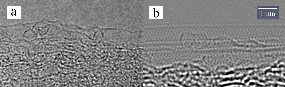
Figure 1: Example for knock-on damage in Single-Wall Carbon-Nanotubes (SWNT) imaged in High-Resolution Transmission Electron Microscopy (HR-TEM, microscope FEI Titan 80-300). (a) after 10 sec electron irradiation at 300keV (b) after 20 min electron irradiation at 80 keV (image from [3]).
The complex damage mechanism of sensitive materials under the electron beam is not fully understood [4]. In order to develop methods to prevent it, further investigation of radiation damage is required. This requirement includes the interaction of the electron beam with the sample, the influence of lens aberrations, and properties of electron source and camera.
Image calculations have become an inevitable tool for the analysis of HR-TEM images, the optimization of imaging conditions, and the refinement of theoretical models for the sample under investigation. Additionally, lowering of the acceleration voltage can be complimented by novel sample-preparation methods. Furthermore, low acceleration voltages have several important advantages for spectroscopic applications, in particular electron energy-loss spectroscopy (EELS) and in-situ microscopy at low voltages is still in its infancy.
Existing developments in low-voltage lower resolution electron microscopy (as by September 2015)
Electron microscopy also allows the fabrication of tabletop-instruments with nm-resolution. These are useful, e.g. for the study of organic surfaces. A very low voltage (< 1 kV), CC/CS-corrected combined Low-Energy Electron Microscope (LEEM) / Photoemission Electron Microscopes (PEEM) has been realized (named SMART) in 2002 [5]. This is equipped with a tetrode mirror corrector and an imaging energy filter providing 2 nm spatial and 0.1 eV energy resolution. The development has been performed by the former group of Harald H. Rose at the TU Darmstadt, the Fritz-Haber-Institute of the Max-Planck-Society in Berlin and the company LEO.
The tabletop instrument FEG 5 kV TEM/STEM/SEM of the company Delong Instruments in Brno, Czech Republic offers another approach for imaging objects at low voltages with a resolution of about one nanometer. The advantages of this instrument are its smallness and simplicity and its strong objective lens (CS = 0.63 mm), which enables a theoretical resolution limit of 0.9 nm. However, the actual instrument achieves only a resolution of about 2.5 nm. This microscope produces good results for organic unstained samples. Because the instrument has no tilt option for the stage, it cannot be applied for most of the material science research [6].
Low-Energy Electron Microscopy (LEEM) has great potential for imaging of low-Z number specimens, in particular organic crystals and surfaces, due to high contrast and extremely low radiation damage. R. Tromp’s group at IBM Research, Yorktown Heights, NY has demonstrated [7] a lateral spatial resolution of 5nm, while resolving vertically single atomic steps (1.36Å on Si (001)). Deleterious charging effects on insulators, a key obstacle for imaging organic material in a LEEM, have been mitigated in a dual beam LEEM [8], where two electron beams with different landing energies or a photon and electron beam are used to compensate charging.
However, to allow the observation of biological objects with the resolution of a HRTEM would imply a revolution in life-sciences in general and biology in particular.
Existing developments in low-voltage high resolution electron microscopy (as by September 2015)
In 2009, the most advanced type of aberration corrector, which corrects chromatic aberration (CC) and spherical aberration (CS), was finalized for the first time for a high resolution transmission electron microscope as a result of a cooperation of the companies CEOS (for the corrector) and FEI (for the microscope column) in the frame of the Transmission Electron Aberration corrected electron Microscope (TEAM) project. This corrector, of which 4 have been installed in HRTEM microscopes today, is optimized for operation between 80 – 300 kV accelerating voltage and allows in principle operation until 50 kV. It reaches a resolution of 0.5 Å at 300 kV [1]. Today, CEOS is the only manufacturer of CC/CS correctors worldwide and the two companies of the first CC/CS corrected microscope project, CEOS and FEI, are cooperating again in the frame of the SALVE project. To correct for lower voltages, the CC/CS corrector needs a completely different design [9].
A transmission electron microscopy project with the aim to realize a CC/CS corrector also for the very low voltage range has been launched in Japan in 2006. This project involves as industry partner the company JEOL and as academic partner the National Institute of Advanced Industrial Science and Technology (AIST) Japan who develop an atomic-resolution TEM/STEM operating at voltages in the range between 30 and 60 kV [10]. During the course of the project, the voltage was even lowered down to 15 kV. Now, the strategy of the company changed and higher resolution at low voltages is performed by the alternative approach for reduction the contribution of the chromatic aberration: using a monochromator to limit the energy spread of the primary electrons in combination with CS correction. The same approach is pursued by the company NION which already offers STEM that are aligned at voltages down to 40 kV [11].
Existing alternative approaches to increase the resolution of beam sensitive objects in electron microscopy (as by September 2015)
The tolerable electron dose which can be applied to beam sensitive materials is often strongly limited. The group of Jannik Meyer in Vienna, Austria carries out research on new statistical methods aimed to reduce radiation damage [12] by distributing the dose over many identical copies of the object.
The structure of electron beam-sensitive materials can today also be observed with Freezing-TEM techniques. Freezing-Microscopes for typical samples as small molecules or molecular complexes embedded in thin layers of vitrified ice (thicknesses typically on the order of 50 – 100 nm) and thicker sections of cellular material and tissue can be imaged with higher resolution as the molecules are stabilized and the electron dose can be increased without damaging the sample. The sample preparation and data evaluation effort is high for this approach.
At Osaka University, Japan, the group of Professor Takai is developing a low-voltage phase-contrast TEM aimed for imaging unstained biological molecules at atomic resolution. Instead hard-ware aberration correction they use a real-time defocus image modulation procedure for posterior numerical compensation of the spherical aberration. This group has already achieved near atomic resolution of DNA at 200 kV [13]. For this method the effort for acquiring an image and for the data evaluation is considerably higher than for hardware correction.
SALVE is a unique research approach in the field of low-voltage TEM, comprising the fields: low-voltage HRTEM, spectroscopy, in-situ TEM, low-voltage TEM imaging theory and outreach. The project consists of topics in experiments, development of theory, sample preparation and instrument development. For the detailed description of SALVE research you can see the interactive SALVE research graph and the content in the section research on this web site.
References
- Erni, R., Rossell, M. D., Kisielowski, C., & Dahmen, U. (2009). Atomic-resolution imaging with a sub-50-pm electron probe. Physical Review Letters, 102: 096101, doi: 10.1103/PhysRevLett.102.096101
- Hartel, P., Mueller, H., Uhlemann, S., Zach, J., & Haider, M., (2010). Benefits of Simultaneous CC-and CS correction. Microscopy and Microanalysis, 16: 114-115, doi: 10.1017/S1431927610055133
- Kaiser U. A., Chuvilin A., Meyer J., Biskupek J. (2009), Microscopy at the bottom. In: W. Grogger, F. Hofer, P. Poelt (Eds.) Materials Science Microscopy Conference MC2009, 3: 1-6, doi: 10.3217/978-3-85125-062-6-379
- Egerton, R. F. (2014). Choice of operating voltage for a transmission electron microscope. Ultramicroscopy, 145: 85-93, doi: 10.1016/j.ultramic.2013.10.019
- Schmidt, Th., U. Groh, R. Fink and E. Umbach, O. Schaff, W. Engel, B. Richter, H. Kuhlenbeck, R. Schlögel, H.-J. Freund and A. M. Bradshaw, D. Preikszas, P. Hartel, R. Spehr and H. Rose, G. Lilienkamp, E. Bauer and G. Benner (2002), XPEEM with energy-filtering: advantages and first results from the SMART project, Surface Review and Letters, 9: 223-232, doi: 10.1142/S0218625X02001811
- Drummy, L. F., J. Yang, D. C. Martin (2004), Low-voltage electron microscopy of polymer and organic molecular thin films, Ultramicroscopy, 99: 247–256, doi: 10.1016/j.ultramic.2004.01.011
- Tromp, R. M., M. Mankos, M. C. Reuter, A. W. Ellis, and M. Copel (1998), A New Low Energy Electron Microscope, Surface Review & Letters, 5: 1189-97, doi: 10.1142/S0218625X98001523
- Mankos, M., V. Spasov, L. Han, S. Kojima, X. Jiang, S. Harb, L. Grella, and C. Czarnik (2008) Low Energy Electron Microscopy for Semiconductor Applications, Mater. Res. Soc. Symp. Proc., 1088E: W03-01, ed. D. L. Adler, E. Bauer, G. L. Kellogg and A. Scholl, doi: 10.1557/PROC-1088-W03-01
- Haider, M., Uhlemann, S., Hartel, P., & Müller, H. (2014). Towards High Resolution in TEM and STEM: What are the Limitations and Achievements. Microscopy and Microanalysis, 20: 378-379, doi: 10.1017/S1431927614003614
- Hosokawa, F., Sawada, H., Kondo, Y., Takayanagi, K., & Suenaga, K. (2013). Development of Cs and Cc correctors for transmission electron microscopy. Microscopy, 62: 23-41, doi: 10.1093/jmicro/dfs134
- Krivanek, O. L. , N. Dellby, M. F. Murfitt, M. F. Chisholm, T. J. Pennycook, K. Suenaga and V. Nicolosi (2010) Gentle STEM: ADF imaging and EELS at low primary energies, Ultramicroscopy, 110: 935-945, doi: 10.1016/j.ultramic.2010.02.007
- Meyer, J. C., Kotakoski, J., & Mangler, C. (2014). Atomic structure from large-area, low-dose exposures of materials: A new route to circumvent radiation damage. Ultramicroscopy, 145: 13-21, doi: 10.1016/j.ultramic.2013.11.010
- Takai Y., T. Nomaguchi, S. Matsushita, and Y. Kimura (2006), Molecular-scale imaging of unstained deoxyribonucleic acid fibers by phase transmission electron microscopy, Applied Physics Letters, 89: 133903, doi: 10.1063/1.2357564