The Sub-Angstrom Low-Voltage Electron Microscopy (SALVE) project: The way to atomic resolution at very low voltages
The Sub-Angstrom Low-Voltage Electron Microscopy (SALVE) project, developed in 2007 and submitted to the German Research Foundation in Spring 2008, aimed to explore, and develop transmission electron microscopy for atomically resolved imaging of thin inorganic and organic materials at low accelerating voltages between 20 kV and 80kV (120kV). The project was divided into three parts: First, SALVE I, a feasibility study conducted from 2009 to 2010. This phase focused on determining the feasibility of building a CC/CS corrected microscope in the 20-80 kV range using the Libra TEM platform from Zeiss and the CS corrector from CEOS. The findings indicated that it is feasible to build a CC/CS corrected microscope operating at lower voltages, even down to 20 kV. Consequently, the SALVE II project, conducted from 2011 to 2015, focused on integrating and adjusting the CC/CS corrector and the high-voltage stages, as well as modifying the base Zeiss Libra TEM to adapt to the lower voltage range and corrector. Third, the SALVE III project, which ran from 2015 to 2017, involved collaboration with FEI, specifically working on the base FEI Titan Themis to adapt it to the 20-80 kV range and to the CC/CS corrector. Concurrently, during SALVE I and II, there was an ongoing evaluation and development of in-situ TEM techniques.
SALVE: Pioneering Low Voltages Electron Microscopy
At the beginning of the 21st century, the most radical advancement that revolutionized the microscopy world in the field of transmission electron microscopy (TEM) was the hardware correction of the spherical aberration (CS) of electron lenses first introduced for medium-ranged electron energies. The introduction of spherical aberration correctors in transmission electron microscopy overcame the fundamental limitations imposed by lens aberrations, significantly enhancing the resolution beyond the previous range of several tenths of a nanometer. As consequence, materials research was brought up to a so far unprecedented level; answering many of the scientific communities so far unsolved questions in science and technology. However, as is so often the case in science, with this achievement new unsolved problems became visible and their solution into reach. Namely atomic imaging with low electron energies for radiation-sensitive thin materials, which were destroyed at higher voltages. Such ideas about the critical interplay between electron beam energy and specimen preservation manifested themselves in two independently developed low-voltage electron microscopy projects, the Triple C project developed by Kazutomo Suenaga (Japan) and the SALVE project developed by Ute Kaiser (Germany).
The projects were specifically designed to enhance the resolution of the electron microscope when operating at low accelerating voltages. Lowering the electron energy effectively reduces beam damage, especially knock-on damage, thereby significantly prolonging the time before harmful beam effects occur. However, at these lower electron energies, aberration correction becomes increasingly essential to attain atomic resolution. [Rose, 2007; Kaiser 2008]. In literature, the first microscopes that used lower voltages operated at 80 kV in CS-corrected TEM [Kujawa et al., 2006, Kaiser 2008] and at 60 kV in CS-corrected Scanning Transmission Electron Microscopy (STEM) [Dellby et al., 2008]. With the reduction of accelerating voltages to thresholds as low as 80 kV and 60 kV a second limitation of the resolution of the electron microscope, a limitation for imaging radiation sensitive materials, was overcome. The recalibration to lower voltages enabled extended observation times for radiation-sensitive specimens without inducing beam damage, thereby allowing for higher specimen resolution despite a lower instrumental resolution [Rose 2009].
Bolstering this strategic shift was the surge in interest in radiation sensitive two-dimensional (2D) materials, such as graphene [Geim and Novoselov 2007] and the demand for methodologies to enable their study at atomic resolution [Meyer et al. 2007] without inducing structural modifications [Krasheninnikov & Banhart 2007]. Indeed, the low-voltage S/TEM was rapidly advancing the research field of graphene and the 2D materials family, as evidenced by a series of breakthrough studies [Gass, et al., 2008; Meyer et al., 2008; Alem et al., 2009; Bar-Sadan et al. 2009, Chuvilin et al., 2009; Enyashin et al., 2009; Girit et al., 2009; Jia et al., 2009; Meyer et al., 2009a,b; Warner, et al., 2009; Chuvilin et al., 2010; Gómez-Navarro et al., 2010; Kotakoski et al., 2010, Krivanek et al., 2010a,b; Suenaga & Koshino, 2010; Wang et al., 2010; Huang, et al., 2011; Jinschek et al., 2011; Liu et al., 2011; Meyer et al., 2011a,b; Park et al., 2011; Urban et al., 2011; Wang et al., 2011; Zan et al., 2011].
Nevertheless, the search for the ideal balance between image resolution and sample preservation continued, as certain materials remained susceptible to electron beam damage at particular sites such as edges and defect sites even at 80 kV and 60 kV [Krasheninnikov & Nordlund 2010]. This impelled the community to further reduce the acceleration voltage down to 50 kV [Barton et al., 2011], 40 kV [Bell et al., 2011; Dellby et al., 2011], 30 kV [Sasaki et al., 2011; Sawada et al., 2011; Suenaga et al., 2011], and finally down to 20 kV [Kaiser et al., 2011]. Each reduction of the accelerating voltage is related to a lower wavelength of the electron and thus provides higher challenges for achieving atomic resolution. In response, researchers adopted innovative strategies to further improve the achieved resolution, including the use of improved electron monochromators with CS-corrected S/TEM, to refine the electron beam's energy width [Hawkes 2009; Bell et al. 2010a,b; Hartel et al., 2010; Kaiser et al. 2011] or the development of high-speed and high-sensitivity complementary metal oxide semiconductor (CMOS) electron detectors [Dahmen et al. 2009], especially for low energies [Faruqi 2009]. Furthermore, time-resolved ultrafast nanodiffraction [Batson 2011] was also shown to contribute to an enhanced image resolution. A next step to solve the resolution problem was to realize CC correction in the low-kV or “gentle” (scanning-) transmission electron microscopy [Rose 2009; Krivanek et al. 2011; Leary & Brydson 2011]. Addressing chromatic aberration emerged as the third pivotal challenge, necessitating sophisticated solutions to preserve atomic resolution.
It was within this complex scientific landscape that the SALVE project was conceived. Its mission was to pioneer a CC/CS–corrector for low-voltage High-Resolution Transmission Electron Microscopy (HRTEM) built on the Carl Zeiss Libra 200 column. This technological leap aimed to facilitate sub-Angstrom resolution at significantly reduced voltages, thereby enabling unprecedented atomic-scale investigations of radiation-sensitive materials. In undertaking this challenge, the SALVE project sought to correct the spherical and the chromatic aberration and thus surmount the third limitation that had constrained electron microscopy of electron beam sensitive materials.
SALVE I: Feasibility study of Chromatic Aberration Correction at low voltages (2009-2010)
SALVE I, the initial phase of the SALVE project, was a feasibility study focused on determining whether it was possible to develop a CC/CS-corrected microscope capable of achieving atomic resolution at operating voltages as low as 20 kV. This endeavor included integrating all necessary components while adhering to the time and budget constraints set by the subsequent phase, SALVE II. The purpose of SALVE I was to lay the groundwork for the development and realization of this advanced CC/CS-corrected microscope.
The Achievements in SALVE I
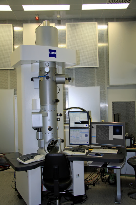
Throughout the SALVE I project, the Zeiss Libra Platform, equipped with the CEOS CS corrector, was utilized. This setup, referred to as the 'SALVE I microscope,' underwent modifications to enable operation at lower voltages, reaching down to 20 kV (refer to Figure 1 for reference). Key enhancements included optimizing the accelerator's design and the Field Emission Gun (FEG) alignment. The objective was to ensure the microscope could operate effectively across a broad voltage range from 20 to 80 kV, without sacrificing brightness. The study involved testing several critical components.
Coma-Free Lens and electron optics: This involved defining requirements for specifications
(focal lengths, operating modes, high-voltage range), corrector interface
requirements, arrangement of apertures and detectors, possibilities for phase
plate integration, options for Scanning Transmission Electron Microscopy
(STEM), Köhler illumination, adjustment concept, tolerance calculations,
mechanical concept, pole pieces (geometry, materials), integration in the
column, integration of additional components (goniometer, apertures,
detectors), magnetic shielding, and vacuum concept (pump cross-sections,
sealing concept).
Cryo-Piezo-Goniometer Feasibility Study: This focused on stability (vibration, drift, positioning
accuracy, repeatability of stored positions), evaluation of mechanical
focusing, cryo aspects (definition of sample carriers, cooling coupling,
possibility of heating the sample), double/rotation-tilt capabilities, and
transfer mechanisms.
Low Voltage Feasibility Study: This involved adjusting the Libra platform for low voltage
(LV), measuring specifications, software adaptation if necessary, filter
studies, investigation of limitations of corrected Omega filter at LV and
across 20-120 kV, measurement of electron optical parameters, possibly
developing an optimized concept for the corrected Omega filter for LV, FEG
studies, stability of electronics, thermal, electromagnetic, acoustic stability
measurements, direct electron detectors, and anamorphic phase plate requirements.
Corrector
Development by CEOS: This involved a feasibility study of adapting the corrector used in the
TEAM project for operation at lower voltages of 20-80 kV, instead of its
original range of 80-300 kV. Initially, the CC/CS corrector from the
TEAM project was thoroughly evaluated to determine its feasibility and
performance at the lower voltage range. To address these challenges, CEOS set a
goal to develop a new corrector system specifically optimized for the 20-80 kV
voltage range dictated by the SALVE project. This involved a detailed
optimization process focusing on both intrinsic and parasitic image errors.
Parasitic image errors, which arise from deviations from the ideal geometry.
The development by CEOS in SALVE I also included the work on CS-Corrected Libra at 20 kV: the adjustment of the CS corrector in the Libra at 20 kV.
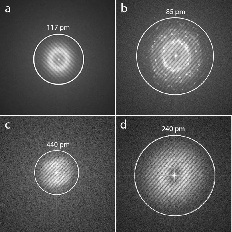
The SALVE I microscope embodied already both technical innovation and operational excellence. For instance, when utilized at 20 kV, the monochromator ensured high image contrast at much higher spatial frequencies [Uhlemann & Haider, 2002]. The microscope's capabilities were further enhanced in 2011 when it received an upgrade that integrated an imaging CEOS CS-corrector (CETCOR). Without the monochromator, the chromatic aberration was limiting the resolution of the SALVE I microscope to 5.2 Å (calculated value for ΔE=0.75 eV from a contrast of 13.5%) [Kaiser et al., 2011]. Operating with the monochromator with a slit width of 2.5 μm (ΔE=170 meV) extended the calculated 13.5%-level to 2.5 Å. The range of Young's fringes measurements at 20 and 80 kV shown in Figure 2 support the calculated values for the information limit of the microscope at 20 kV determined by the combination of image spread and focus spread [Haider et al., 2010]. The focus spread limit, which comprises the effect of the chromatic aberration and other focus instabilities could be reduced from 5 Å without monochromator to 2.5 Å with a reduced energy width of 0.17 eV. The experimentally discerned 1% levels at 20 kV correspond to a value of 2.5 Å/1.23, approximately 2.0 Å. This is in good agreement with theory, as Young's fringes are always visible beyond the calculated 1/e2-level. “visibility” in a diffractogram is related to a contrast level of about 1%, which is at a factor of 1.23 times higher spatial frequency than the 1/e2-level [Haider et al., 2010]. The image spread limit of the instrument was shown to be better than 1.8 Å by applying an illumination tilt of 30 mrad in combination with Young's fringes [Kaiser et al., 2011], see Figure 2.
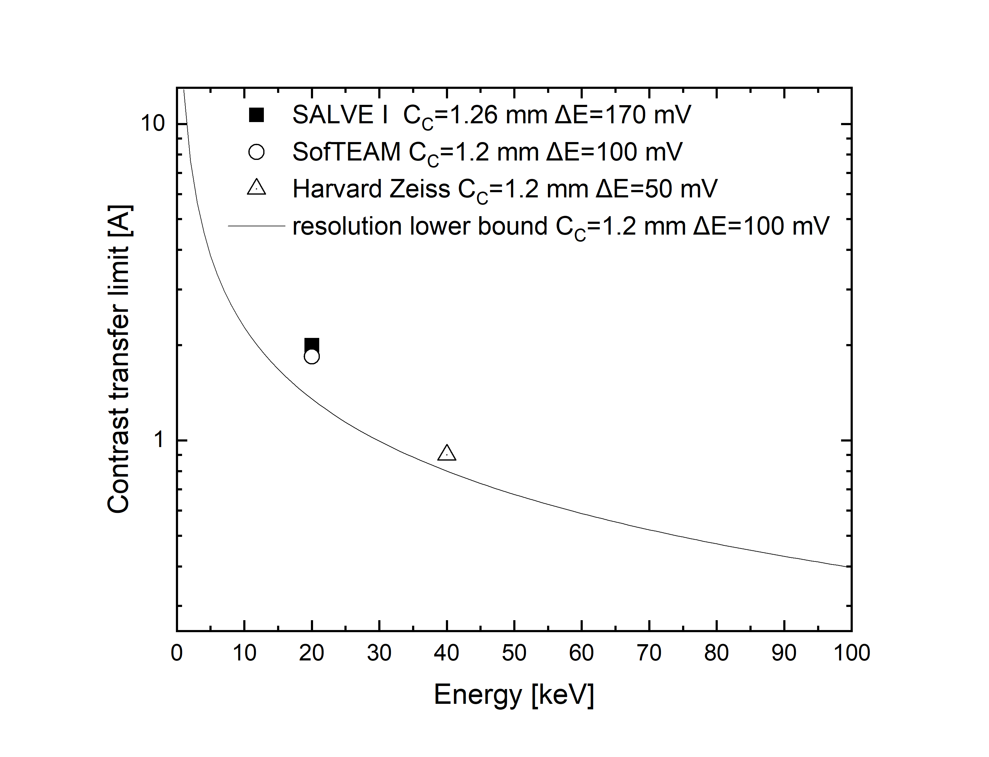
The pursuit of atomic resolution was thus found to be crucial at 20 kV. Supplementary insights obtained from model simulations during the SALVE I project validated that enhancing the contrast markedly at extremely low accelerating voltages cannot be realized by merely correcting spherical aberration and implementing monochromation but also requires reduction or correction of the chromatic aberration coefficient [Lee et al. 2012]. Also, further results from the literature support these finding: Bell's research determined that already at an operating voltage of 40 kV a 1% threshold was achieved at 0.9 Å in Young's fringes experiment utilizing the CS-corrected, monochromated Zeiss Libra TEM [Bell et al., 2012]. Kisielowski et al. found the 1% level of the Young’s fringes experiment was at 1.84 Å at an energy spread of 100 meV in the electron beam and an aberration coefficient of 1.2 mm in the CS-corrected monochromated TEAM0.5 instrument at 20 kV (SofTEAM) [Barton et al., 2012]. A similar contrast transfer limit was found for the Triple C #1 instrument. At 15 kV, the 1% level of the Young’s fringes experiment was at 2.0 Å at an energy spread of 270 meV in the electron beam and an aberration coefficient of 0.52 mm [Sasaki et al., 2014]. Figure 3 shows the three experimental data points for the 1% level of the the Young’s fringes experiment together with theoretical predictions of the information limit boundary dictated by chromatic aberration [Bell et al., 2012]. The empirical finding harmonizes well with emphasizing the paramount importance of chromatic aberration correction, particularly when operating at lower accelerating voltages.
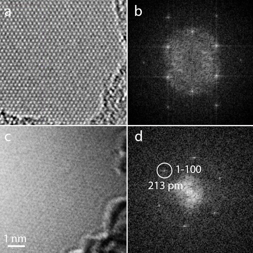
To validate the obtained results with the Youngs fringes experiments at 20 and 80 kV with practically relevant samples, graphene was used as a test specimen and imaged with the SALVE I microscope at 20 and 80 kV, see Figure 4. The images captured showcased the ability to delineate frequencies up to the first-order reflections in graphene at 213 pm even at 20 kV [Kaiser et al., 2011]. The much lower resolution of the CS-corrected, monochromated TEM image at 20 kV compared to 80 kV underscored the strong dependence of the CC-limited probe size on the primary energy and the need for developing practical CC-correctors [Krivanek et al., 2011] or novel designs of monochromators optimized for very low voltages [Morishita et al. 2016] as the next step in aberration-corrected S/TEM that are designed to operate at very low voltages [Börrnert et al., 2023].
SALVE I ensured a robust CS aberration-corrected TEM platform for in-depth application-related experiments, from real-time in-situ observations to the study of the effects of spherical and chromatic aberration. It validated the feasibility of constructing a CC/CS aberration-corrected TEM for operation at low voltages [Kaiser et al., 2011]. During the experiments conducted in SALVE I, the impact of monochromation at 80 kV was observed to be relatively minimal, a finding that is consistent with the scholarly literature of the time. [Warner et al., 2012] found that several HRTEM imaging reports of graphene, with monochromation [Meyer et al., 2008] and without [Warner et al., 2009] at 80 kV exhibited only minor differences in image resolution. However, findings from SALVE I, in line with existing literature, underscored the necessity of employing a CS corrector and reducing the accelerating voltage to 60 or 80 kV—particularly for radiation-sensitive materials—to attain atomic resolution. It was discussed in the community that existing microscopes that were typically operating at medium accelerating voltages could undergo modifications to support lower voltages and additionally be equipped with a CS correctors to enable atomic resolution imaging of many radiation-sensitive materials [Börrnert et al. 2013].
Below 60 kV, chromatic aberration becomes the prevailing factor that progressively impairs resolution. Achieving atomic resolution grows increasingly challenging, even with the utilization of both monochromators and CS correctors. For instance, when we consolidate the findings from the CS-corrected and monochromatic Zeiss Libra TEMs at Harvard University and from Ulm University's SALVE I project, we observe a resolution of 110 pm at 40 kV and 250 pm at 20 kV. These empirical values align well with the theoretically computed resolution constraints attributable to chromatic aberration, even when a monochromator is in use [Bell et al., 2012; Kaiser et al., 2011]. Consequently, to attain atomic resolution at extremely low voltages, such as 20 kV, the application of CC-correction becomes essential in conjunction with CS correction and monochromation.
Prior to the initiation of the SALVE I project, there was a debate regarding the definition of 'low voltage' within the context of transmission electron microscopy. This discussion was settled following a pivotal study [Meyer et al., 2012], which demonstrated minimal knock-on damage in graphene at 80 kV, with damage significantly increasing at 90 kV. These findings were instrumental in establishing a globally accepted standard within the SALVE project, defining 'low voltage' at 80 kV and any voltage below.
SALVE II: Unraveling the Potential of Chromatic Aberration Correction at low voltages (2011-2015)
In February 2011, the SALVE project entered its second phase, marking a significant advancement in electron microscopy. This was initiated with an official ceremony at Ulm University where the project received the combined endorsement of the German Research Foundation (DFG) and the Baden Württemberg Ministry for Science, Research and Art (MWK). Notably, Professor Josef Zweck of the German Society for Electron Microscopy (DGE) recognized the project's potential as a pivotal advancement for high-resolution transmission electron microscopy. SALVE II was one of the most notable periods of the SALVE project, spanning from 2011 to 2015. This phase represented a pinnacle of technological advancement in electron microscopy, with achievements and challenges that played a foundational role in the project's trajectory. After the feasibility of CC/CS-corrected TEM at low voltages (20-80 kV) had been positively evaluated in SALVE I, the focus shifted to the creation of a novel fully corrected electron microscope capable of operating at low voltages.
The Achievements in SALVE II
After the possibility of realizing a CC/CS-corrected TEM with atomic resolution at low primary energies (20-80 kV) has been positively evaluated in SALVE I, the development phase SALVE II was started aiming at creating the microscope. The immediate quantifiable achievements during the initial phase of SALVE II included:
- Aberration correction for axial aberrations up to the 5th order
- Correction of off-axial aberrations up to the 3rd order
- A large, distortion-free field of view due to corrections for anisotropic magnification
- Fine-tuning of the 3rd order spherical aberration and defocus to achieve the desired phase contrast.
- The technology underlying the CC/CS corrector was further exemplified by its software showcasing the versatility and depth of aberration measurement capabilities.
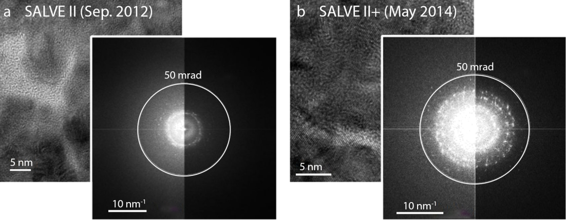
While the journey was marked by successes, challenges were also faced. One notable discovery was the impact of the Johnson-Nyquist-noise in electron optical elements on resolution [Uhlemann et al., 2013; Reich 2013]. Initially, this resulted in a limited atom contrast of the test material graphene for the SALVE II microscope, showing 2% contrast in September 2012, see Figure 6a.
From Zeiss Libra SALVE II to Zeiss Libra SALVE II+: Lowering the Nyquist-Johnson Noise in the TEM
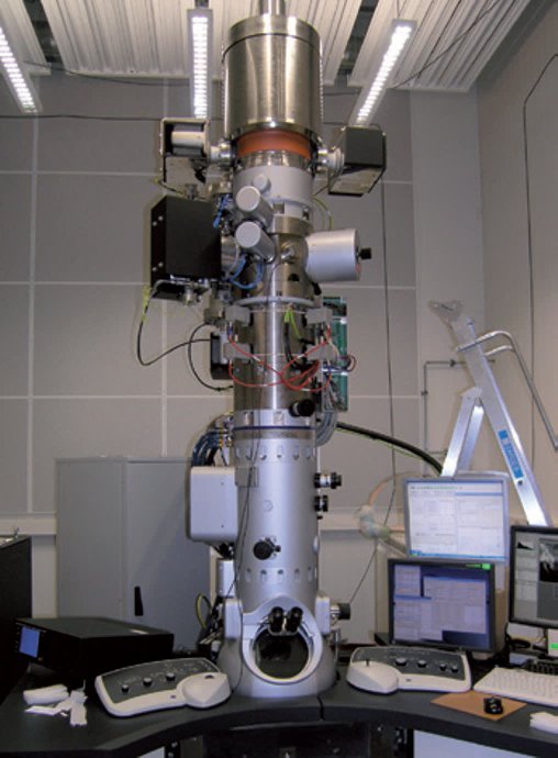
The core of SALVE II's accomplishments revolved around the development of the CC/CS corrector. Designed by CEOS and based on the concepts by Rose and Kuhn (Rose, 1992; Rose, 1992), the corrector was primed to adjust and align for optimal phase contrast imaging. The result was an instrument capable of controlling all relevant aberrations, thus ensuring aberration-free imaging with an extensive field of view. The corrector was integrated in the Zeiss Libra based SALVE II microscope with the aim of achieving less complexity in the microscope's construction, minimized length, and optimal optical quality, see Figure 5.
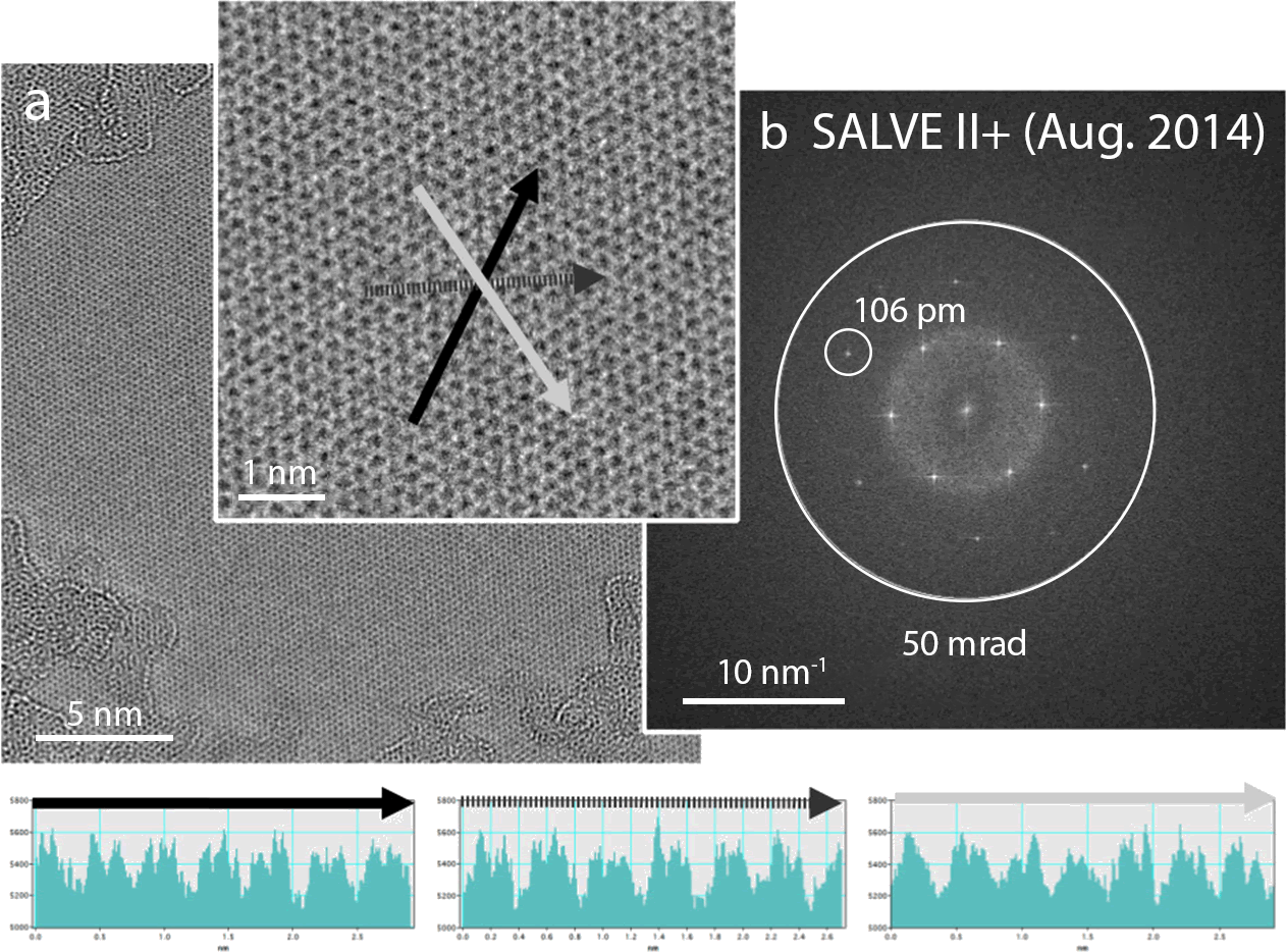
Understanding and the innovative redesigning of the corrector's electron optical components pushed the boundaries of resolution. Tests at CEOS GmbH in Heidelberg on the upgraded corrector for the chromatic aberration corrected PICO-instrument of the research center Jülich (CCOR+) had already shown that the effect of Johnston-Nyquist-noise can be significantly reduce by a reduction of the beam diameter in the corrector accompanied by an increase of the magnetic and electric field strengths. The increase of the electric field strengths of the multipoles from 5 to 8 kV is necessary to maintain their correction power. The strength of the magnetic multipoles was increased accordingly in the SALVE corrector. These measures have reduced the image spread caused by the corrector from 35 pm to 25 pm at 80 kV. The instrument with the improved corrector was named SALVE II+. It had a total image spread of the corrector of 25 pm and of the Zeiss Libra column of 25 pm. In August 2014, measurements with SALVE II+ convincingly showed that the electron optical design enables phase contrast imaging with a hitherto not-existing quality, see Figure 6b.
The phase contrast image of a graphene test specimen taken at 80 kV showed a remarkable total image spread of corrector and instrument together of 35 pm at 80 kV. Contrast transfer was shown up to about 8% above background and frequency transfer until 106 pm, see Figure 7.
The phase contrast image of a graphene test specimen taken at 80 kV showed a remarkable total image spread of corrector and instrument together of 35 pm at 80 kV. Contrast transfer was shown up to about 8% above background and frequency transfer until 106 pm, see Figure 7.
Image simulations performed during SALVE II on the example of graphene and silicon showed that the influence of inelastic scattering at 20 kV, especially on low-Z materials, is significant. A large usable aperture, allowed by the corrector technology of SALVE II, provides not only improved resolution but also enhanced contrast [Lee et al., 2013]. Furthermore, studies examined the relationship between electron dose, signal-to-noise ratio, atom contrast, and resolution, introducing a dose-dependent contrast metric and determining the best samplings for varying electron dose conditions [Lee et al., 2014].
However, SALVE II also met unforeseen challenges. One significant setback was the withdrawal of the Carl Zeiss Company from the TEM market in January 2013, which threatened the completion of the project phase. This potential derailment was navigated with the onboarding of a new TEM manufacturer - FEI company. SALVE II's Zeiss Libra-based instrument continued to serve for application-related experiments until September 2013 and for corrector development until August 2014. With the new TEM manufacturer on board, a third project phase was created that included the realization of a CC/CS-corrected TEM with the company FEI
In summary, the
SALVE II phase of the SALVE project witnessed both immense progress and faced
significant challenges. The development and success of the CC/CS-corrector,
despite setbacks, solidified SALVE II's position as an important period in
electron microscopy. The innovative approach to overcome challenges,
particularly in understanding the Johnson-Nyquist-noise. With the new TEM
manufacturer on board, the creation of a third project phase that included the
realization of a CC/CS-corrected TEM with the company
FEI, ensured that the project could be completed as planned.
Highlighted Topics
Concluding Remarks on SALVE II
In summary, the SALVE II phase of the SALVE project witnessed both immense progress and faced significant challenges. The development and success of the CC/CS-corrector, despite setbacks, solidified SALVE II's position as an epoch-making period in electron microscopy. The innovative approach to overcome challenges, particularly in understanding the Johnson-Nyquist-noise. With the new TEM manufacturer on board, the creation of a third project phase that included the realization of a CC/CS-corrected TEM with the company FEI, ensured that the project could be completed as planned.
SALVE III: Realizing Chromatic Aberration Correction at low voltages (2015-2017)
In the development of aberration-corrected transmission electron microscopy (TEM), the SALVE (Sub-Ångström Low Voltage Electron microscopy) project has undoubtedly marked its presence as one of the major milestones, in particular because of the final successes and advancements achieved in the third phase (SALVE III). SALVE III, or the Production Phase, spanned the period from 2015 to the end of 2017, marking the inclusion of the FEI company in the SALVE project after the withdrawal of ZEISS. The primary focus of this phase was the enhancement and integration of the quadrupole-octupole CC/ CS-corrector by CEOS into the FEI Titan Themis TEM, which had originally been developed in SALVE II.
The achievements in SALVE III
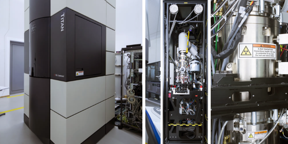
The SALVE III microscope was notably developed to meet rigorous criteria for low-voltage operations. Special modifications were implemented, ranging from the CC-corrector to components such as an improved vacuum system, cryo shields, and more stable specimen holders. The result was a TEM system that surpassed the performance of the Titan Themis, particularly tailored for low-voltage microscopy applications, see Figure 8.
By the year 2016, reports confirmed that the focus spread of the SALVE III microscope was essentially zero, even when the electron beam had an energy width of 350 meV [Linck et al., 2016]. This was significant in opening doors to atomic-resolution imaging for materials sensitive to high-energy electron beams, which is monumental in the field of electron microscopy as aberrations are minimal, allowing for sharp phase contrast imaging between 55 and 67 mrad, see Figure 9. The experimental information limit measured using Young’s fringes method was 76 pm at 80 kV, 83 pm at 60 kV, 90 pm at 40 kV, 115 pm at 30 kV and 139 pm at 20 kV. As the electron wavelength is 6 pm at 40 kV, the SALVE project achieved a resolution limit as minuscule as 15 wavelengths at 40 kV - a new world record.
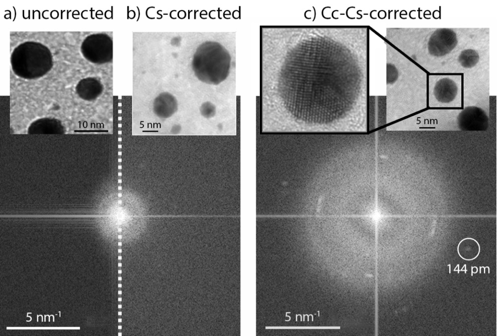
In a direct comparison using gold nanoislands (NIs) as test specimens, it was observed that the combined chromatic and spherical aberration corrections in the SALVE III enable true atomic resolution within gold islands at 20 kV, see Figure 10c. This is evident from the presence of the Au [022] reflections in the diffractogram, corresponding to a lattice spacing of 144 pm.
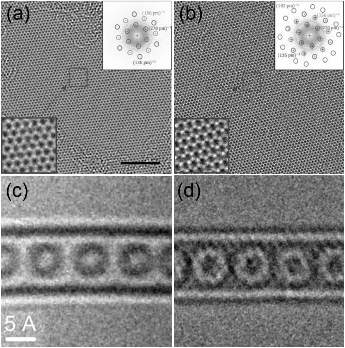
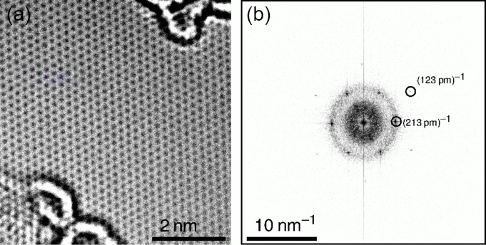
When observing 2D MoS2 at 30 kV, the resolution achieved with the CC/CS-corrected SALVE III microscope is roughly twice that of standard CS-corrected microscopes operating at 80 kV, as illustrated in Figure 11 a,b. The 80 kV CS-corrected FEI Titan image reveals information transfer up to 135 pm. In contrast, the 30 kV CC/CS-corrected SALVE III micrograph presents a more pronounced reflection and transferred information at higher frequencies, reaching up to 102 pm for the atomic honeycomb lattice of 2D molybdenum disulfide. This improved resolution is also evident in the case of C60 buckyballs, as shown in Figure 11 c,d. Individual atoms within the buckyball structure remain elusive when viewed under the 80 kV CS-corrected FEI Titan. Yet, with the CC/CS-corrected SALVE III TEM, not only is atomic resolution attainable, but it also provides the capability to study dynamics atom-by-atom at 30 kV. For graphene, information transfer was confirmed up to at least 123 pm at 20 kV, see Figure 12.
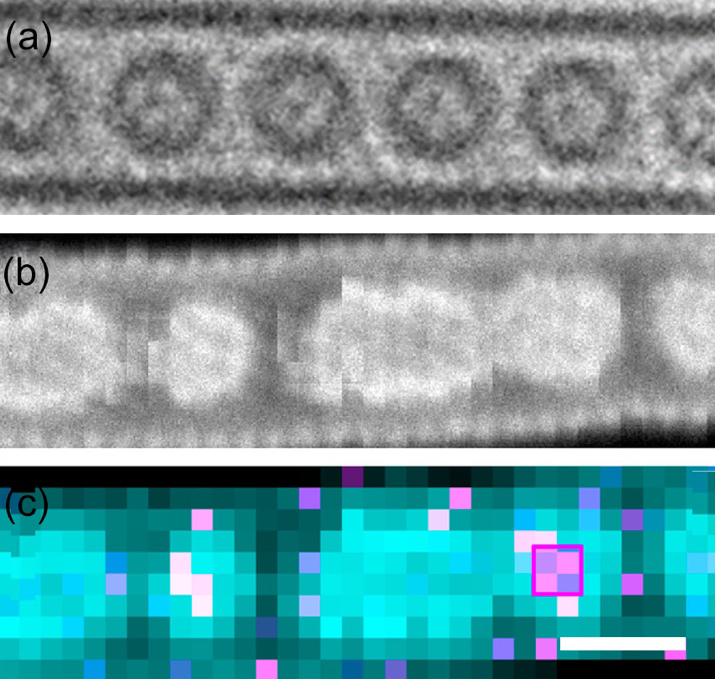
The data of SALVE III was analyzed together and compared with the data from the SuperSTEM microscope, see Figure 13 [Biskupek et al., 2020]. HF and H2O molecules were encapsulated within a fullerene inside a single-walled carbon nanotube (X@C60)@SWNT. The combined microscopic analysis demonstrated that electron beams break H–F or H–O bonds in real-time, releasing hydrogen and leaving fluorine or oxygen, with fluorine being more stable inside the fullerene.
SALVE III,
supported by the combined efforts of CEOS GmbH, FEI Company, and Ulm
University, marked a new step in the progress of imaging of beam-sensitive
materials by electron microscopy [Kisielowski et al. 2015, Chen et al. 2020]. Achieving
resolutions at 40 kV equivalent to only 15 times the electron wavelength set
new benchmarks in phase-contrast TEM imaging. The correction of chromatic
aberration further expanded opportunities in analytical imaging, with large
energy windows almost uniformly focused on the image plane. SALVE III not only
met but exceeded expectations, paving the way for advanced materials analysis
on sensitive specimens, for instance, low-D materials or biological specimens.
The SALVE III research project marked significant progress in addressing several critical challenges inherent in enhancing transmission electron microscopy (TEM) resolution. Key achievements included: (i) minimizing Johnson noise in CC-corrected microscopes, (ii) implementing chromatic aberration correction at ultra-low voltages, specifically down to 20 kV, and (iii) attaining an exceptional information limit, such as 144 pm for gold nanoparticles on thin carbon film and lattice reflections up to 123 pm for graphene, both at 20 kV or 107 pm for graphene and 102 pm for MoS2 at 30 kV, or a groundbreaking experimental information limit defined by the 13.5% level of the Youngs fringes experiment ranging from 0.76 Å - 1.40 Å across the 20–80 kV range. Before the advancements made in SALVE III, attaining true atomic resolution at such low voltages was near impossible due to chromatic aberration. SALVE III broke through this barrier, achieving and contributed to the task of building of keener microscopes that are needed urgently to solve current challenges [Pennycook et al. 2014]. It has set a new benchmark in transmission electron microscopy (TEM) resolution at ultra-low voltages.
Highlighted Topics
Summary and outlook of the SALVE project
The SALVE project played a pivotal role in pioneering measurements and simulations of the knock-on threshold across a variety of 2D materials, e.g. molybdenum disulfide (MoS2) [Komsa et al., 2013, Lehnert et al., 2017, Kretschmer et al., 2020]. These studies underscored the necessity of having access to atomic resolution across a wide energy range, extending down to 20 kV, to mitigate knock-on damage effectively. A notable example is the behavior of MoS2 under irradiation; for instance it was observed that radiation damage related to single sulfur vacancies intensifies significantly when the accelerating voltage is increased beyond 55 kV [Speckmann et al., 2023].
Today, the SALVE III microscope has already contributed to numerous studies at 20 kV [Skowron et al., 2017, Kabiri, et al., 2019], 30 kV [Biskupek et al., 2020, Jordan et al. 2021, Köster et al., 2022], 40 kV [Lehnert et al., 2019, Köster et al., 2021] 60 kV [Norman et al., 2021, Cull et al., 2023], and 80 kV [Kühne et al., 2018, Neumann et al., 2019, Kuzmany et al., 2021] at atomic resolution. A straightforward method to measure electron source brightness and illumination semi-angle distribution in transmission electron microscopy was introduced [Börrnert et al., 2018]. During SALVE III, the imaging of biological samples with the TEM was further explored [Majorovits et al., 2016]. The SALVE III microscope demonstrated a resolution of 2.4 Å at 20 kV for the most radiation sensitive, biological samples [Kabiri, et al., 2019]. Atomic resolution was even achieved for di- and triatomic molecules [Biskupek et al., 2020]. Using the SALVE III microscope, the dynamics of Re2 molecules were imaged, revealing changes in Re–Re bond lengths and identifying a previously unknown bonding state with a bond order less than one [Cao et al., 2020].
The understanding of beam damage is important for exploring new ways for engineering and modifying materials by electron beams [Zhao et al., 2017]. The possibility of tuning the electron energy with the SALVE III microscope down to 20 kV by maintaining atomic resolution enabled the study of beam damage processes on the single atom level and significantly advanced the understanding of the radiation damage mechanisms in the electron microscope [Kretschmer et al., 2020].
New imaging
modes for radiation sensitive specimen were further explored [Ophus et al., 2016]. The annular differential phase
contrast (ADPC) mode in scanning transmission electron microscopy (STEM) offers
superior image contrast and atomic-level resolution at 30 kV compared to
traditional methods. This advancement may allow for studying thick samples'
inner structures without slicing them [Lee et al.,
2019].
Despite these advancements, post-project analysis has
highlighted specific areas that require further exploration to continue
evolving TEM resolution capabilities. These future challenges encompass: (i) expanding the range of accelerating voltages (20-300 kV)
within which a single CC-corrector can effectively neutralize
chromatic aberration, especially given the extensive energy range of
contemporary monochromated, CS-corrected TEMs, e.g., see ref. [Kaiser et al., 2019, Börrnert et al., 2023], to cover
a wide range of materials, (ii) further reducing Johnson Noise, which continues
to compromise the electron microscope's resolution, e.g. see ref. [Axelrod et al., 2023], (iii) addressing the high
costs associated with CC-correctors, e.g. see ref. [Zaluzec et al., 2015, Dunin-Borkowski &
Houben, 2016], (iv) simplifying the intricate
calibration and alignment procedures required for CC correctors,
e.g. see ref. [Haider
et al., 2008, Kaiser et al., 2011, SALVE website – CC correction
realized], (v) managing the stringent stability requirements for
magnetic and electric fields in CC-corrected microscopes,
necessitating specialized and costly microscope rooms, e.g. see ref. [CEOS website – Atomic resolution for everybody, SALVE
website - SALVE 3 TEM moves to the new building, Taurino
& Carlino, 2023,], and (vi) tackling the
limitation imposed by the 20 kV minimum acceleration voltage, which is above
the knock-on threshold for extremely light elements like hydrogen, e.g. see
ref. [Skowron et al., 2017, Subatki et al.,
2023]. This last point is particularly vital as one of the ongoing
challenges lies in imaging 2D materials with minimal electron beam damage, e.g.
see ref. [Kisielowski et al., 2021],
potentially necessitating even further reductions in accelerating voltages.
Looking ahead, the focus in the field is shifting toward the innovation of more advanced monochromator systems optimized for very low voltages [Morishita et al., 2016]. This advancement is poised to be the next significant step for commercially available CS-corrected S/TEMs at very low voltages, promising atomic resolution without the necessity for intricate handling through CC-correction software. Furthermore, a monochromator has a double purpose in S/TEM, it is also improving the performance of electron energy loss spectroscopy (EELS) experiments. Highlighting this trend, CEOS has proposed a pioneering design for a ground-potential monochromator tailored for CS-corrected STEM from 300 kV down to 30 kV [Börrnert et al., 2023]. In a practical application of advanced technology, the JEOL NEOARM STEM, a current model equipped with the newly developed CEOS ASCOR two-hexapole corrector, has demonstrated remarkable capabilities in resolution. This CS-corrected and monochromated microscope could discern lattice reflections as fine as 73 pm in silicon and up to 93 pm in molybdenum disulfide (MoS2) at an accelerating voltage of 60 kV [Sagawa et al., 2022].
References
Alem, N., Erni, R., Kisielowski, C., Rossell, M. D., Gannett, W., & Zettl, A. J. P. R. B. (2009). Atomically thin hexagonal boron nitride probed by ultrahigh-resolution transmission electron microscopy. Physical review B, 80, 155425, https://doi.org/10.1103/PhysRevB.80.155425
Axelrod, J. J., Petrov, P. N., Zhang, J. T., Remis, J., Buijsse, B., Glaeser, R. M., & Müller, H. (2023). Overcoming resolution loss due to thermal magnetic field fluctuations from phase plates in transmission electron microscopy. Ultramicroscopy, 249, 113730, https://doi.org/10.1016/j.ultramic.2023.113730
Batson, P. E. (2011). Unlocking the time resolved nature of electron microscopy. Proceedings of the National Academy of Sciences, 108, 3099, https://doi.org/10.1073/pnas.1019562108
Bar Sadan, M., Heidelmann, M., Houben, L., & Tenne, R. (2009). Inorganic WS2 nanotubes revealed atom by atom using ultra-high-resolution transmission electron microscopy. Applied Physics A, 96, 343, https://doi.org/10.1007/s00339-009-5208-0
Barton, B., Song, C., & Kisielowski, C. (2011). Atomic resolution at 50-300 kV obtained using low dose rate HRTEM. Microscopy and Microanalysis, 17, 1266, https://doi.org/10.1017/S1431927611007203
Barton, B., Jiang, B., Song, C., Specht, P., Calderon, H., & Kisielowski, C. (2012). Atomic resolution phase contrast imaging and in-line holography using variable voltage and dose rate. Microscopy and Microanalysis, 18, 982, https://doi.org/10.1017/S1431927612001213
Bell, D. C., Russo, C., Meyer, S., Benner, G., & Haider, M. (2010b). Advantages of Monochromated Low Voltage Aberration Corrected TEM. Microscopy and Microanalysis, 16, 118, https://doi.org/10.1017/S1431927610060976
Bell, D. C., Russo, C. J., & Benner, G. (2010b). Sub-Ångström low-voltage performance of a monochromated, aberration-corrected transmission electron microscope. Microscopy and Microanalysis, 16, 386, https://doi.org/10.1017/S1431927610093670
Bell, D., Kolmykov, D., & Russo, C. (2011). Low-Voltage (40 kV) Aberration-Corrected, Monochromated, Imaging for Carbon Nanostructures. Microscopy and Microanalysis, 17, 1490, https://doi.org/10.1017/S1431927611008324
Bell, D. C., Russo, C. J., & Kolmykov, D. V. (2012). 40 kV atomic resolution TEM. Ultramicroscopy, 114, 31, https://doi.org/10.1016/j.ultramic.2011.12.001
Bell, D. C., Mankin, M., Day, R. W., & Erdman, N. (2014). Successful application of low voltage electron microscopy to practical materials problems. Ultramicroscopy, 145, 56, https://doi.org/10.1016/j.ultramic.2014.03.005
Biskupek, J., P. Hartel, M. Haider, & U. A. Kaiser (2012), Effects of residual aberrations explored on single-walled carbon nanotubes. Ultramicroscopy, 116, 1, https://doi.org/10.1016/j.ultramic.2012.03.008
Biskupek, J., Skowron, S. T., Stoppiello, C. T., Rance, G. A., Alom, S., Fung, K. L., Whitby, R. J., Levitt, M. H., Ramasse, Q. M., Kaiser, U. A., Besley, E. & Khlobystov, A. N. (2020) Bond Dissociation and Reactivity of HF and H2O in a Nano Test Tube. ACS Nano, 14, 11178, https://doi.org/10.1021/acsnano.0c02661
Börrnert, F., Uhlemann, S., Müller, H., Gerheim, V., & Haider, M. (2023). A novel ground-potential monochromator design. Ultramicroscopy, 253, 113805, https://doi.org/10.1016/j.ultramic.2023.113805
Börrnert, F., & Kaiser, U. (2018). Chromatic-and geometric-aberration-corrected TEM imaging at 80 kV and 20 kV. Physical Review A, 98, 023861, https://doi.org/10.1103/PhysRevA.98.023861
Börrnert, F., Renner, J., & Kaiser, U. (2018). Electron Source Brightness and Illumination Semi-Angle Distribution Measurement in a Transmission Electron Microscope. Microscopy and Microanalysis, 24, 249, https://doi.org/10.1017/S1431927618000223
Börrnert, F., Bachmatiuk, A., Gorantla, S., Wolf, D., Lubk, A., Büchner, B., & Rümmeli, M. H. (2013). Retro‐fitting an older (S) TEM with two Cs aberration correctors for 80 kV and 60 kV operation. Journal of microscopy, 249, 87, https://doi.org/10.1111/j.1365-2818.2012.03684.x
Cao, K., Skowron, S. T., Biskupek, J., Stoppiello, C. T., Leist, C., Besley, E., Khlobystov, A. N. & Kaiser, U. (2020). Imaging an unsupported metal–metal bond in dirhenium molecules at the atomic scale. Science Advances, 6, eaay5849, https://doi.org/10.1126/sciadv.aay5849
CEOS website – SALVE: CC/CS corrector for the TEM (low-kV range): https://www.ceos-gmbh.de/en/produkte/temcorrectors/salve & Atomic resolution for everybody: https://www.ceos-gmbh.de/en/research/revolution
Chen, Q., Dwyer, C., Sheng, G., Zhu, C., Li, X., Zheng, C., & Zhu, Y. (2020). Imaging beam‐sensitive materials by electron microscopy. Advanced Materials, 32, 1907619, https://doi.org/10.1002/adma.201907619
Chuvilin, A., Bichoutskaia, E., Gimenez-Lopez, M. C., Chamberlain, T. W., Rance, G. A., Kuganathan, N., Biskupek, J., Kaiser, U., & Khlobystov, A. N. (2011). Self-assembly of a sulphur-terminated graphene nanoribbon within a single-walled carbon nanotube. Nature materials, 10, 687, https://doi.org/10.1038/nmat3082.
Chuvilin, A., Kaiser, U., Bichoutskaia, E., Besley, N. A., & Khlobystov, A. N. (2010). Direct transformation of graphene to fullerene. Nature chemistry, 2, 450, https://doi.org/10.1038/nchem.644.
Chuvilin, A., Meyer, J. C., Algara-Siller, G., & Kaiser, U. (2009). From graphene constrictions to single carbon chains. New Journal of Physics, 11, 083019, https://doi.org/10.1088/1367-2630/11/8/083019
Cull, W. J., Skowron, S. T., Hayter, R., Stoppiello, C. T., Rance, G. A., Biskupek, J., Kudrynskyi, Z. R., Kovalyuk, Z. D., Allen, C. S., Slater, T. J. A., Kaiser, U., Patané, A., & Khlobystov, A. N. (2023). Subnanometer-wide indium selenide nanoribbons. ACS nano, 17, 6062, https://doi.org/10.1021/acsnano.3c00670
Dahmen, U., Erni, R., Radmilovic, V., Ksielowski, C., Rossell, M. D., & Denes, P. (2009). Background, status and future of the transmission electron aberration-corrected microscope project. Philosophical Transactions of the Royal Society A: Mathematical, Physical and Engineering Sciences, 367, 3795, https://doi.org/10.1098/rsta.2009.0094
Dellby, N., Bacon, N. J., Hrncirik, P., Murfitt, M. F., Skone, G. S., Szilagyi, Z. S., & Krivanek, O. L. (2011). Dedicated STEM for 200 to 40 keV operation. The European Physical Journal-Applied Physics, 54, 33505, https://doi.org/10.1051/epjap/2011100429
Dellby, N., Murfitt, M., Krivanek, O. L., Kociak, M., March, K., Tence, M., & Colliex, C. (2008). Atomic-resolution STEM at 60 kV primary voltage. Microscopy and Microanalysis, 14(S2), 136, https://doi.org/10.1017/S1431927608088399
Dunin-Borkowski, R. E., & Houben, L. (2016). Spherical and chromatic aberration correction for atomic-resolution liquid cell electron microscopy. Liquid Cell Electron Microscopy, 434, https://doi.org/10.1017/9781316337455.022
Egerton, R. F. (2012). Mechanisms of radiation damage in beam‐sensitive specimens, for TEM accelerating voltages between 10 and 300 kV. Microscopy research and technique, 75, 1550, https://doi.org/10.1002/jemt.22099
Enyashin, A. N., Bar-Sadan, M., Sloan, J., Houben, L., & Seifert, G. (2009). Nanoseashells and nanooctahedra of MoS2: routes to inorganic fullerenes. Chemistry of materials, 21, 5627, https://doi.org/10.1021/cm9021326
Faruqi, A. R. (2009). Principles and prospects of direct high resolution electron image acquisition with CMOS detectors at low energies. Journal of Physics: Condensed Matter, 21, 314004, https://doi.org/10.1088/0953-8984/21/31/314004
Gass, M. H., Bangert, U., Bleloch, A. L., Wang, P., Nair, R. R., & Geim, A. K. (2008). Free-standing graphene at atomic resolution. Nature nanotechnology, 3, 676, https://doi.org/10.1038/nnano.2008.280.
Geim, A. K., & Novoselov, K. S. (2007). The rise of graphene. Nature materials, 6, 183, https://doi.org/10.1038/nmat1849
Girit, Ç. O., Meyer, J. C., Erni, R., Rossell, M. D., Kisielowski, C., Yang, L., Park, C.-H., Crommie, M. F., Cohen, M. L., Louei, S. G., & Zettl, A. (2009). Graphene at the edge: stability and dynamics. Science, 323, 1705, https://doi.org/10.1126/science.11669
Golla-Schindler, U., Algara-Siller, G., Orchowski, A., Wu, Y., Weil, T., & Kaiser, U. (2012). First results of 20 kV EFTEM of core-shell QDS with an albumin-derived polypeptide surface coating on graphene. In: EMC 2012 15th European Microscopy Congress, 16-21 September 2012, Manchester, United Kingdom
Gómez-Navarro, C., Meyer, J. C., Sundaram, R. S., Chuvilin, A., Kurasch, S., Burghard, M., Kern, K., & Kaiser, U. (2010). Atomic structure of reduced graphene oxide. Nano letters, 10, 1144, https://doi.org/10.1021/nl9031617
Haider, M., Uhlemann, S., Schwan, E., Rose, H., Kabius, B., & Urban, K. (1998). Electron microscopy image enhanced. Nature, 392, 768, https://doi.org/10.1038/33823
Haider, M., Müller, H., Uhlemann, S., Zach, J., Loebau, U., & Hoeschen, R. (2008). Prerequisites for a CC/CS-corrected ultrahigh-resolution TEM. Ultramicroscopy, 108, 167, https://doi.org/10.1016/j.ultramic.2007.07.007
Haider, M., Hartel, P., Müller, H., Uhlemann, S., & Zach, J. (2010). Information transfer in a TEM corrected for spherical and chromatic aberration. Microscopy and Microanalysis, 16, 393-408, https://doi.org/10.1017/S1431927610013498
Hartel, P., Müller, H., Uhlemann, S., Zach, J., & Haider, M. (2010). Benefits of simultaneous Cc-and Cs-correction. Microscopy and Microanalysis, 16, 114, https://doi.org/10.1017/S1431927610055133.
Hawkes, P. W. (2009). Aberration correction past and present. Philosophical Transactions of the Royal Society A: Mathematical, Physical and Engineering Sciences, 367, 3637, https://doi.org/10.1098/rsta.2009.0004
Huang, P. Y., Ruiz-Vargas, C. S., Van Der Zande, A. M., Whitney, W. S., Levendorf, M. P., Kevek, J. W., Garg, S., Alden, J. S., Hustedt, C. J., Zhu, Y., Park, J., McEuen, P. L., & Muller, D. A. (2011). Grains and grain boundaries in single-layer graphene atomic patchwork quilts. Nature, 469, 389, https://doi.org/10.1038/nature09718
Jia, X., Hofmann, M., Meunier, V., Sumpter, B. G., Campos-Delgado, J., Romo-Herrera, J. M., Son, H., Hsieh, Y.-P., Reina, A., Kong, J., Terrones, M., & Dresselhaus, M. S. (2009). Controlled formation of sharp zigzag and armchair edges in graphitic nanoribbons. Science, 323, 1701 https://doi.org/10.1126/science.11668
Jinschek, J. R., Yucelen, E., Calderon, H. A., & Freitag, B. (2011). Quantitative atomic 3-D imaging of single/double sheet graphene structure. Carbon, 49, 556, https://doi.org/10.1016/j.carbon.2010.09.058
Jordan, J. W., Fung, K. L., Skowron, S. T., Allen, C. S., Biskupek, J., Newton, G. N., Kaiser, U., & Khlobystov, A. N. (2021). Single-molecule imaging and kinetic analysis of intermolecular polyoxometalate reactions. Chemical Science, 12, 7377, https://doi.org/10.1039/D1SC01874D
Kabiri, Y., Ravelli, R.B.G., Lehnert, T., Qi, H., Katan, A. J., Roest, N., Kaiser, U., Dekker, C., Peters, P. J. & Zandbergen, H. (2019) Visualization of unstained DNA nanostructures with advanced in-focus phase contrast TEM techniques. Scientific reports, 9, 7218, https://doi.org/10.1038/s41598-019-43687-5
Kabius, B., Hartel, P., Haider, M., Müller, H., Uhlemann, S., Loebau, U., J. Zach, & Rose, H. (2009). First application of CC-corrected imaging for high-resolution and energy-filtered TEM. Journal of electron microscopy, 58, 147, https://doi.org/10.1093/jmicro/dfp021
Kaiser, U., Biskupek, J., Meyer, J. C., Leschner, J., Lechner, L., Rose, H., Stöger-Pollach, M., Khlobystov, A. N., Hartel, P., Müller, H., Haider, M., Eyhusen, S., & Benner, G. (2011). Transmission electron microscopy at 20 kV for imaging and spectroscopy. Ultramicroscopy, 111, 1239, https://doi.org/10.1016/j.ultramic.2011.03.012
Kaiser, U., Chuvilin, A., Schröder, R. R., Haider, M., & Rose, H. (2008). Sub-Ångstrøm Low-Voltage Electron Microscopy—future reality for deciphering the structure of beam-sensitive nanoobjects? In: EMC 2008 14th European Microscopy Congress, 1: 35, https://doi.org/10.1007/978-3-540-85156-1_18
Kaiser, U. & Stöger-Pollach, M. (2014). Foreword to the special issue low-voltage electron microscopy. Ultramicroscopy, 145, 1, https://doi.org/10.1016/j.ultramic.2014.05.002
Kaiser, U. (2016). Properties of low-dimensional electron-beam-sensitive objects by spherical and chromatic aberration-corrected low-voltage high-resolution transmission electron microscopy and spectroscopy. In: The 15th European Microscopy Congress (John Wiley & Sons, Germany, 2016): 8679, https://doi.org/10.1002/9783527808465.EMC2016.8679
Kaiser, U. (2019). Imaging and Spectroscopy of Low-Dimensional Low-Z Materials by 20-300 kV TEM. Microscopy and Microanalysis, 25, 1726, https://doi.org/10.1017/S143192761900936X
Kim, J. S., Borisenko, K. B., Nicolosi, V., & Kirkland, A. I. (2011). Controlled radiation damage and edge structures in boron nitride membranes. ACS nano, 5, 3977, https://doi.org/10.1021/nn2005443.
Kirkland, A. I., Saxton, W. O., & Chand, G. (1997). Multiple beam tilt microscopy for super resolved imaging. Journal of electron microscopy, 46, 11, https://doi.org/10.1093/oxfordjournals.jmicro.a023486
Kisielowski, C. (2015). Observing atoms at work by controlling beam–sample interactions. Advanced Materials, 27, 5838, https://doi.org/10.1002/adma.201500082
Kisielowski, C., Specht, P., Rozeveld, S. J., Kang, J., Fielitz, A. J., Barton, D., Salazar, A. C., Dubon, O. D., Van Dyck, D., & Yancey, D. F. (2021). Modulating electron beam–sample interactions in imaging and diffraction modes by dose fractionation with low dose rates. Microscopy and Microanalysis, 27, 1420-1430, https://doi.org/10.1017/S143192762101268X
Komsa, H. P., Kurasch, S., Lehtinen, O., Kaiser, U., & Krasheninnikov, A. V. (2013). From point to extended defects in two-dimensional MoS2: Evolution of atomic structure under electron irradiation. Physical Review B, 88, 035301, https://doi.org/10.1103/PhysRevB.88.035301
Köster, J., Ghorbani-Asl, M., Komsa, H. P., Lehnert, T., Kretschmer, S., Krasheninnikov, A. V., & Kaiser, U. (2021). Defect Agglomeration and Electron-Beam-Induced Local-Phase Transformations in Single-Layer MoTe2. The Journal of Physical Chemistry C, 125, 13601, https://doi.org/10.1021/acs.jpcc.1c02202
Köster, J., Storm, A., Ghorbani-Asl, M., Kretschmer, S., Gorelik, T. E., Krasheninnikov, A. V., & Kaiser, U. (2022). Structural and chemical modifications of few-layer transition metal phosphorous trisulfides by electron irradiation. The Journal of Physical Chemistry C, 126, 15446, https://doi.org/10.1021/acs.jpcc.2c03800
Kotakoski, J., Jin, C. H., Lehtinen, O., Suenaga, K., & Krasheninnikov, A. V. (2010). Electron knock-on damage in hexagonal boron nitride monolayers. Physical Review B, 82, 113404, https://doi.org/10.1103/PhysRevB.82.113404
Krasheninnikov, A. V., & Banhart, F. J. N. M. (2007). Engineering of nanostructured carbon materials with electron or ion beams. Nature materials, 6, 723, https://doi.org/10.1038/nmat1996
Krasheninnikov, A. V., & Nordlund, K. (2010). Ion and electron irradiation-induced effects in nanostructured materials. Journal of Applied Physics, 107, 071301, https://doi.org/10.1063/1.3318261
Kretschmer, S., Lehnert, T., Kaiser, U., & Krasheninnikov, A. V. (2020). Formation of defects in two-dimensional MoS2 in the transmission electron microscope at electron energies below the knock-on threshold: the role of electronic excitations. Nano letters, 20, 2865, https://doi.org/10.1021/acs.nanolett.0c00670
Krivanek, O. L., Chisholm, M. F., Dellby, N., & Murfitt, M. F. (2011). Atomic-resolution STEM at low primary energies. Scanning Transmission Electron Microscopy, 615, https://doi.org/10.1007/978-1-4419-7200-2_15
Krivanek, O. L., Chisholm, M. F., Nicolosi, V., Pennycook, T. J., Corbin, G. J., Dellby, N., Murfitt, M. F., Own, C. S., Szilagyi, Z. S., Oxley, M. P., Pantelides, S. T., & Pennycook, S. J. (2010a). Atom-by-atom structural and chemical analysis by annular dark-field electron microscopy. Nature, 464, 571, https://doi.org/10.1038/nature08879
Krivanek, O. L., Dellby, N., Murfitt, M. F., Chisholm, M. F., Pennycook, T. J., Suenaga, K., & Nicolosi, V. (2010b). Gentle STEM: ADF imaging and EELS at low primary energies. Ultramicroscopy, 110, 935, https://doi.org/10.1016/j.ultramic.2010.02.007.
Kühne, M., Börrnert, F., Fecher, S., Ghorbani-Asl, M., Biskupek, J., Samuelis, D., Krasheninnikov,, A. V., Kaiser, U. & Smet, J. H. (2018). Reversible superdense ordering of lithium between two graphene sheets. Nature, 564, 234, https://doi.org/10.1038/s41586-018-0754-2
Kujawa, S., Erni, R., Freitag, B., Tiemeijer, P., & Stekelenburg, M. (2006). High Resolution TEM at 80 kV Acceleration Voltage – Is Approaching 1 Angstrom Possible? Microscopy and Microanalysis, 12, 1470, https://doi.org/10.1017/S143192760606572X
Kuzmany, H., Shi, L., Martinati, M., Cambré, S., Wenseleers, W., Kürti, J., Koltai, J., Kukucska, G., Cao, K., Kaiser, U., Saito, T. & Pichler, T. (2021) Well-defined sub-nanometer graphene ribbons synthesized inside carbon nanotubes. Carbon, 171, 221, https://doi.org/10.1016/j.carbon.2020.08.065
Leary, R., & Brydson, R. (2011). Chromatic aberration correction: the next step in electron microscopy. In: Advances in Imaging and Electron Physics, 165, 73, https://doi.org/10.1016/B978-0-12-385861-0.00003-8
Lechner, L., Biskupek, J., & Kaiser, U. A. (2012). Improved Focused Ion Beam Target Preparation of (S)TEM Specimen — A Method for Obtaining Ultrathin Lamellae. Microscopy and Microanalysis, 18, 379, https://doi.org/10.1017/S1431927611012499
Lee, Z., Meyer, J. C., Rose, H., & Kaiser, U. (2012), Optimum HRTEM image contrast at 20 kV and 80 kV - Exemplified by graphene. Ultramicroscopy, 112, 39, https://doi.org/10.1016/j.ultramic.2011.10.009
Lee, Z., Rose, H., Hambach, R., Wachsmuth, P., & Kaiser, U. (2013), The influence of inelastic scattering on EFTEM images – exemplified at 20 kV for graphene and silicon. Ultramicroscopy, 134, 102, https://doi.org/10.1016/j.ultramic.2013.05.020
Lee, Z., Rose, H., Lehtinen, O., Biskupek, J., & Kaiser, U. (2014). Electron dose dependence of signal-to-noise ratio, atom contrast and resolution in transmission electron microscope images. Ultramicroscopy, 145, 3, https://doi.org/10.1016/j.ultramic.2014.01.010
Lee, Z., Kaiser, U., & Rose, H. (2019). Prospects of annular differential phase contrast applied for optical sectioning in STEM. Ultramicroscopy, 196, 58, https://doi.org/10.1016/j.ultramic.2018.09.012
Lehnert, T., Biskupek, J., Köster, J., Linck, M., & Kaiser, U. (2016). Quantitative low‐voltage spherical and chromatic aberration‐corrected high‐resolution TEM analysis of beam‐specimen interactions in single‐layer MoS2 and MoS2/graphene heterostructures. In: The 15th European Microscopy Congress, 5742, https://doi.org/10.1002/9783527808465.EMC2016.5738
Lehnert, T., Lehtinen, O., Algara–Siller, G., & Kaiser, U. (2017). Electron radiation damage mechanisms in 2D MoSe2. Applied Physics Letters, 110, 033106, https://doi.org/10.1063/1.4973809
Lehnert, T., Ghorbani-Asl, M., Köster, J., Lee, Z., Krasheninnikov, A. V., & Kaiser, U. A. (2019). Electron-Beam-Driven Structure Evolution of Single-Layer MoTe2 for Quantum Devices. ACS Appl. Nano Mater., 5, 3262, https://doi.org/10.1021/acsanm.9b00616
Linck, M., Hartel, P., Uhlemann, S., Kahl, F., Müller, H., Zach, J., Haider, M., Niestadt, M., Bischoff, M., Biskupek, J., Leez, Z., Lehnert, T., Börrnert, F., Rose, H., & Kaiser, U. (2016). Chromatic aberration correction for atomic resolution TEM imaging from 20 to 80 kV. Physical Review Letters, 117, 076101, https://doi.org/10.1103/PhysRevLett.117.076101
Liu, Z., Suenaga, K., Wang, Z., Shi, Z., Okunishi, E., & Iijima, S. (2011). Identification of active atomic defects in a monolayered tungsten disulphide nanoribbon. Nature communications, 2, 213, https://doi.org/10.1038/ncomms1224
Majorovits, E., Angert, I., Kaiser, U., & Schröder, R. R. (2016). Benefits and Limitations of Low-kV Macromolecular Imaging of Frozen-Hydrated Biological Samples. Biophysical Journal, 110, 776, https://doi.org/10.1016/j.bpj.2016.01.023
Meyer, J. C., Geim, A. K., Katsnelson, M. I., Novoselov, K. S., Booth, T. J., & Roth, S. (2007). The structure of suspended graphene sheets. Nature, 446, 60, https://doi.org/10.1038/nature05545
Meyer, J. C., Kisielowski, C., Erni, R., Rossell, M. D., Crommie, M. F., & Zettl, A. (2008). Direct imaging of lattice atoms and topological defects in graphene membranes. Nano letters, 8, 3582, https://doi.org/10.1021/nl801386m
Meyer, J., Chuvilin, A., & Kaiser, U. (2009a). Electron microscopic studies with graphene. Microscopy and Microanalysis, 15, 126, https://doi.org/10.1017/S1431927609096056
Meyer, J. C., Chuvilin, A., Algara-Siller, G., Biskupek, J., & Kaiser, U. (2009b). Selective sputtering and atomic resolution imaging of atomically thin boron nitride membranes. Nano letters, 9, 2683, https://doi.org/10.1021/nl9011497
Meyer, J. C., Kurasch, S., Park, H. J., Skakalova, V., Künzel, D., Groß, A., Chuvilin, A., Algara-Siller, G., Roth, S., Iwasaki, T., Starke, U., Smet, J. H., & Kaiser, U. (2011). Experimental analysis of charge redistribution due to chemical bonding by high-resolution transmission electron microscopy. Nature materials, 10, 209, https://doi.org/10.1038/nmat2941
Meyer, J. C., F. Eder, S. Kurasch, V. Skakalova, J. Kotakoski, H.-J. Park, S. Roth, A. Chuvilin, S. Eyhusen, G. Benner, A. V. Krasheninnikov, U. A. Kaiser (2012). Accurate Measurement of Electron Beam Induced Displacement Cross Sections for Single-Layer Graphene. Physical Review Letters, 108: 196102, https://doi.org/10.1103/PhysRevLett.108.196102
Morishita, S., Mukai, M., Suenaga, K., & Sawada, H. (2016). Atomic resolution imaging at an ultralow accelerating voltage by a monochromatic transmission electron microscope. Physical Review Letters, 117, 153004, https://doi.org/10.1103/PhysRevLett.117.153004
Muller, D. A. (2009). Structure and bonding at the atomic scale by scanning transmission electron microscopy. Nature materials, 8, 263, https://doi.org/10.1038/nmat2380
Neumann, C., Kaiser, D., Mohn, M. J., Füser, M., Weber, N. E., Reimer, O., Gölzhäuser, A., Weimann, T., Terfort, A., Kaiser, U., & Turchanin, A. (2019). Bottom-up synthesis of graphene monolayers with tunable crystallinity and porosity. ACS nano, 13, 7310, https://doi.org/10.1021/acsnano.9b03475
Norman, L. T., Biskupek, J., Rance, G. A., Stoppiello, C. T., Kaiser, U., & Khlobystov, A. N. (2022). Synthesis of ultrathin rhenium disulfide nanoribbons using nano test tubes. Nano Research, 15, 1282, https://doi.org/10.1007/s12274-021-3650-2
O’Keefe, M. A., Hetherington, C. J. D., Wang, Y. C., Nelson, E. C., Turner, J. H., Kisielowski, C., Malm, J.-O., Mueller, R., Ringnalda, J., Pan, M., & Thust, A. (2001). Sub-Angstrom high-resolution transmission electron microscopy at 300 keV. Ultramicroscopy, 89, 215, https://doi.org/10.1016/S0304-3991(01)00094-8
Ophus, C., Ciston, J., Pierce, J., Harvey, T. R., Chess, J., McMorran, B. J., Czarnik, C., Rose, H. H., & Ercius, P. (2016). Efficient linear phase contrast in scanning transmission electron microscopy with matched illumination and detector interferometry. Nature Communications, 7, 10719, https://doi.org/10.1038/ncomms10719
Park, H. J., Meyer, J., Roth, S., & Skákalová, V. (2010). Growth and properties of few-layer graphene prepared by chemical vapor deposition. Carbon, 48, 1088, https://doi.org/10.1016/j.carbon.2009.11.030
Pennycook, S. J., & Kalinin, S. V. (2014). Microscopy: Hasten high resolution. Nature, 515, 487, https://doi.org/10.1038/515487a
Reich, E. S. (2013). Imaging hits noise barrier. Nature 499, 135, https://doi.org/10.1038/499135a
Rose, H. H. (2009). Future trends in aberration-corrected electron microscopy. Philosophical Transactions of the Royal Society A: Mathematical, Physical and Engineering Sciences, 367, 3809, https://doi.org/10.1098/rsta.2009.0062.
Rose, H. H. (2007). Criteria and prospects for realizing optimum electron microscopes. Microscopy and Microanalysis, 13, 134, https://doi.org/10.1017/S1431927607071358
Rose, H. (1992). Prospects of aberration corrected TEM. In: 10th Eur. Congr. El. Micr. (Granada, Spain), 47
Rose, H. (1992). Electron optical correction system for lenses of electron microscope. Patent, DE4204512 A1
Rose, H. (1971). Properties of spherically corrected achromatic electron lenses: Spherically corrected electron lenses with improved resolving capacity and aberration compensation. Optik, 33, 1-24.
Sagawa, R., Yasuhara, A., Hashiguchi, H., Naganuma, T., Tanba, S., Ishikawa, T., Riedel, T., Hartel, P., Linck, M., Uhlemann, S., Müller, H., & Sawada, H. (2022). Exploiting the full potential of the advanced two-hexapole corrector for STEM exemplified at 60kV. Ultramicroscopy, 233, 113440, https://doi.org/10.1016/j.ultramic.2021.113440
SALVE center website – SALVE 1-3 project: http://www.salve-project.de/home.html; SALVE CS/CC correction realized: https://www.salve-project.de/newspress/SALVE-CC-correction-realized.html; SALVE 3 TEM moves to the new building: https://www.salve-project.de/newspress/SALVE-microscope-comes-home.html
Sasaki, T., Sawada, H., Hosokawa, F., Shimizu, Y., Nakamichi, T., Yuasa, S., Kawazie, M., Kaneyama, T., Kondo, Y., Kimoto, K., & Suenaga, K. (2011). Performance and application of chromatic/spherical aberration-corrected 30 kV transmission electron microscope. Microscopy and Microanalysis, 17, 1530, https://doi.org/10.1017/S143192761100852X
Sasaki, T., Sawada, H., Nakamichi, T., Hosokawa, F., Omoto, K., Tomita, T., Kaneyama, T., Kondo, Y., Kimoto, K., & Suenaga, K. (2009). Performance of low-voltage electron microscope with new aberration correction system and cold field emission gun. Microscopy and Microanalysis, 15, 1080, https://doi.org/10.1017/S1431927609094057
Sawada, H., Hosokawa, F., Sasaki, T., Yuasa, S., Kawazoe, M., Terao, M., Kaneyama, T., Kondo, Y., Kimoto, K., & Suenaga, K. (2011). Development of 30-kV CC/CS correction tandem system. Microscopy and Microanalysis, 17, 1184, https://doi.org/10.1017/S1431927611006799
Sasaki, T., Sawada, H., Hosokawa, F., Sato, Y., & Suenaga, K. (2014). Aberration-corrected STEM/TEM imaging at 15 kV. Ultramicroscopy, 145, 50, https://doi.org/10.1016/j.ultramic.2014.04.006
Schmidt, T., Groh, U., Fink, R., Umbach, E., Schaff, O., Engel, W., Richter, B., Kuhlenbeck, H., Schlögl, R., Freund, H.-J., Bradshaw, A. M., Preikszas, D., Hartel, P., Spehr, R., Rose, H., Lilienkamp, G., Bauer, E., & Benner, G. (2002). XPEEM with energy-filtering: advantages and first results from the SMART project. Surface Review and Letters, 9, 223, https://doi.org/10.1142/S0218625X02001811
Schröder, R. R., Barton, B., Rose, H., & Benner, G. (2007). Contrast enhancement by anamorphotic phase plates in an aberration corrected TEM. Microscopy and Microanalysis, 13, 8, https://doi.org/10.1017/S1431927607074867
Skowron, S. T., Chamberlain, T. W., Biskupek, J., Kaiser, U., Besley, E., & Khlobystov, A. N. (2017). Chemical Reactions of Molecules Promoted and Simultaneously Imaged by the Electron Beam in Transmission Electron Microscopy. Accounts of Chemical Research, 50, 1797, https://doi.org/10.1021/acs.accounts.7b00078
Speckmann, C., Lang, J., Madsen, J., Monazam, M. R. A., Zagler, G., Leuthner, G. T., McEvoy, N., Mangler, C., Sui, T., & Kotakoski, J. (2023). Combined electronic excitation and knock-on damage in monolayer MoS2. Physical Review B, 107, 094112, https://doi.org/10.1103/PhysRevB.107.094112
Subakti, S., Daqiqshirazi, M., Wolf, D., Linck, M., Kern, F. L., Jain, M., Kretschmer, S., Krasheninnikov, A. V., Brumme, T., & Lubk, A. (2023). Electron holographic mapping of structural reconstruction at mono-and bilayer steps of h−BN. Physical Review Research, 5, 033137, https://doi.org/10.1103/PhysRevResearch.5.033137
Suenaga, K., & Koshino, M. (2010). Atom-by-atom spectroscopy at graphene edge. Nature, 468, 1088, https://doi.org/10.1038/nature09664
Suenaga, K., Iizumi, Y., & Okazaki, T. (2011). Single atom spectroscopy with reduced delocalization effect using a 30 kV-STEM. The European Physical Journal-Applied Physics, 54, 33508, https://doi.org/10.1051/epjap/2011100414
Taurino, A., & Carlino, E. (2023). The Relevance of Building an Appropriate Environment around an Atomic Resolution Transmission Electron Microscope as Prerequisite for Reliable Quantitative Experiments: It Should Be Obvious, but It Is a Subtle Never-Ending Story! Materials, 16, 1123, https://doi.org/10.3390/ma16031123
Uhlemann, S., & Haider, M. (2002). Experimental set-up of a fully electrostatic monochromator for a 200 kV TEM. In: Proc. 15th Int. Cong. Electr. Micr., 3, 327, https://doi.org/10.1017/S1431927602105861
Uhlemann, S., Müller, H., Hartel, P., Zach, J., & Haider, M. (2013). Thermal magnetic field noise limits resolution in transmission electron microscopy. Physical Review Letters, 111, 046101, https://doi.org/10.1103/PhysRevLett.111.046101
Urban, K. W. (2015). In quest of perfection in electron optics: A biographical sketch of Harald Rose on the occasion of his 80th birthday. Ultramicroscopy, 151, 2, https://doi.org/10.1016/j.ultramic.2014.12.002
Urban, K. W. (2011). The challenges of graphene. Nature materials, 10, 165, https://doi.org/10.1038/nmat2964, HRTEM image of graphene at 80 kV originally from Jinschek et al. 2011.
Wang, Z., Li, H., Liu, Z., Shi, Z., Lu, J., Suenaga, K., Joung, S.-K., Okazaki, T., Gu, Z., Zhou, J., Gao, Z., Li, G., Sanvito, S., Wang, E., & Iijima, S. (2010). Mixed low-dimensional nanomaterial: 2D ultra narrow MoS2 inorganic nanoribbons encapsulated in quasi-1D carbon nanotubes. Journal of the American Chemical Society, 132, 13840, https://doi.org/10.1021/ja1058026
Wang, Z., Zhao, K., Li, H., Liu, Z., Shi, Z., Lu, J., Suenaga, K., Joung, S.-K., Okazaki, T., Jin, Z., Gu, Z., Gao, Z., & Iijima, S. (2011). Ultra-narrow WS2 nanoribbons encapsulated in carbon nanotubes. Journal of Materials Chemistry, 21, 171, https://doi.org/10.1039/C0JM02821E
Warner, J. H., Rümmeli, M. H., Ge, L., Gemming, T., Montanari, B., Harrison, N. M., Büchner, B., & Briggs, G. A. D. (2009). Structural transformations in graphene studied with high spatial and temporal resolution. Nature nanotechnology, 4, 500, https://doi.org/10.1038/nnano.2009.194
Warner, J. H., Margine, E. R., Mukai, M., Robertson, A. W., Giustino, F., & Kirkland, A. I. (2012). Dislocation-driven deformations in graphene. Science, 337, 209, https://doi.org/10.1126/science.1217529
Zaluzec, N. J. (2015). The influence of CS/CC correction in analytical imaging and spectroscopy in scanning and transmission electron microscopy. Ultramicroscopy, 151, 240, https://doi.org/10.1016/j.ultramic.2014.09.012
Zan, R., Bangert, U., Ramasse, Q., & Novoselov, K. S. (2011). Imaging of Bernal stacked and misoriented graphene and boron nitride: experiment and simulation. Journal of microscopy, 244, 152, doi: 10.1111/j.1365-2818.2011.03520.x
Zhao, X., Kotakoski, J., Meyer, J. C., Sutter, E., Sutter, P., Krasheninnikov, A. V., Kaiser, U., & Zhou, W. (2017). Engineering and modifying two-dimensional materials by electron beams. MRS Bulletin, 42, 667, https://doi.org/10.1557/mrs.2017.184

