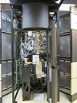
FEI joins University of Ulm and CEOS in SALVE project research collaboration
The Sub-Ångström Low Voltage Electron (SALVE) microscope will improve contrast and reduce damage on bio-molecules and two dimensional nanomaterials such as graphene.
March, 16th 2015 - FEI (NASDAQ: FEIC) announced today that it has entered into an agreement with Germany’s University of Ulm and Heidelberg-based CEOS GmbH to develop a sub-Ångström low-voltage electron microscope, in the frame of Uni-Ulm’s SALVE project. The collaboration will involve the development of a dedicated aberration-corrected transmission electron microscope (TEM) that is capable of imaging radiation-sensitive materials, such as two-dimensional (2D) and organic materials, and selected molecules, with molecular or even atomic-scale resolution. The TEM is also expected to provide spectroscopic information at very low acceleration voltages.
“Current-generation TEMs typically operate at high voltages of up to 300kV, which provides limited contrast and destroys radiation-sensitive samples before they can be imaged,” states Trisha Rice, vice president and general manager of Materials Science at FEI. “The SALVE project is focused on designing a TEM that can operate at accelerating voltages as low as 20 kV, enabling it to provide new structural and spectroscopic information of samples, which previously could not be imaged because they would be destroyed at the higher voltages.”
CEOS, the company with long-year expertise in corrected electron optical systems, focuses in the frame of SALVE on developing new optimized corrector technology to compensate for the chromatic and spherical aberration at low voltages. FEI will be developing the TEM system itself, which will be based on a Titan™ 80-300 TEM platform, one of the world’s first and most powerful commercial aberration-corrected microscopes. While the University of Ulm is working on application-related development, including sample preparation methods and the theory of imaging with low-energetic electrons.
"The SALVE project, promoted by the German Research Foundation (DFG) and the Ministry of Science, Research and the Arts Baden-Württemberg Germany, started in 2008 and progress has been made," states the project leader Ute Kaiser, Electron Microscopy Group of Materials Science, University of Ulm. "We greatly appreciate that FEI has stepped in to build on these developments after their so successful projects in the past." The first resolution improvement by a factor of 2 from 0.24 nm to 0.13 nm was realized for a Cs-corrected 200 kV FEI-TEM in 1998 [1] and the second resolution improvement to 65 pm at 300 kV was realized for a CC-CS-corrected 80 - 300 kV FEI-S/TEM in 2010 [2]. In tradition of these pioneer projects, we investigate with the SALVE project together with FEI and CEOS the next generation of aberration corrected high-resolution TEMs now with very low voltages down to 20 kV and bring the SALVE project to its final phase. The keys to success will be the ability to correct optical aberrations, the stability of the microscope platform and the microscope room, and progress in sample preparation and contrast interpretation. As scientists, we hardly can wait to operate our new microscope and to see what kinds of ground-breaking discoveries we might possibly be able to achieve; very much in the light of Otto Scherzer, a German physicist and pioneer in the work on theoretical and practical aberration correction, who recognized the need to reduce radiation damage in the electron microscope already 45 years ago [3].
Max Haider, CEOS, adds, “The SALVE project involves the use of low accelerating voltages, which have been rarely used in electron microscopes to date. We have had great success with our spherical aberration correctors on FEI’s Titan platform, and we would like to extend that capability to correct the chromatic aberration that dominates at low voltages. This new microscope could open up entirely new fields in materials science that involves investigating materials that have been impossible to study with existing microscope technology.”
-
Haider, M., Uhlemann, S., Schwan, E., Rose, H., Kabius, B., & Urban, K. (1998). Electron microscopy image enhanced. Nature 392: 768-769, doi: 10.1038/33823
-
Haider, M., Hartel, P., Muller, H., Uhlemann, S., & Zach, J. (2010). Information transfer in a TEM corrected for spherical and chromatic aberration. Microscopy and Microanalysis, 16: 393-408, doi: 10.1017/S1431927610013498
-
Scherzer, O. (1970). Die Strahlenschädigung der Objekte als Grenze für die hochauflösende Elektronenmikroskopie. Berichte der Bunsengesellschaft für physikalische Chemie 74: 1154-1167, doi: 10.1002/bbpc.19700741113

