A new two-dimensional graphitic semiconductor: Carbon nitride
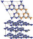
A European team of chemists and physicists, including Gerardo Algara-Siller and Ute Kaiser from the SALVE project at the University of Ulm has discovered a new two-dimensional graphitic semiconductor [1]. The existence of a "graphitic carbon nitride" (g-C3N4) was suggested already in earlier works [2-5], however the atomic structure still was not unravelled yet. The novel material, ‘triazine-based graphitic carbon nitride’ (TGCN) was predicted theoretically in 1996 [6], and thanks to low-voltage aberration-corrected transmission electron microscopy it could now be unraveled from these experiments for the first time. Our graphitic carbon nitride (see Fig. 1) belongs - as graphene - to the new class of two-dimensional materials but instead of having a 0 eV band gap it exhibits a direct band gap of 1.6 - 2.0 eV.
Currently still the most commonly used semiconducting material for modern electronics and solar cells is silicon, but it is expensive and its sources are limited. In principle, abundant organic and two-dimensional materials might replace silicon for certain applications. In general, graphene has a very desirable combination of high carrier mobility, high current stability, heat stability and thermal conductivity [7-9]. But the semi metallic nature of graphene and the lack of a band gap have prevented the development of a graphene-based switch [10]. Although with certain physical and chemical modifications a band gap could be opened in graphene [11-14], simpler methods for silicon-free switches are to use inherent semiconductors. A field effect transistor with MoS2 (band-gap = 1.8 eV) can be prepared, but MoS2 has known chemical limitations [15-16]. It is therefore desirable to extend the graphene system with another two-dimensional material with inherent semiconductor properties. Starting from the inexpensive molecule dicyandiamide, the science team of this publication prepared and analysed crystals of graphitic carbon nitride, a two-dimensional layered material consisting of carbon and nitrogen.
The team was coordinated by Michael Bojdys, experimental chemist and postdoctoral researcher in the department of Andrew Cooper in Liverpool. Professor Cooper said “This was not a planned output of our EPSRC Programme Grant. The great thing about this funding scheme is that it allows flexibility, which also allowed us to link to the various European partners that made the research possible.”
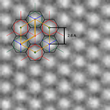
An important part of the structural characterisation and identification of the grown material was high-resolution low-voltage transmission electron microscopy. In Fig. 2 the experimental microcraph shows the hexagonal 2D honeycomb structure. Using this information, the team found that the structure agrees with the historical model of g-C3N4 (unit cell of 2,6 A), which is composed of staggered layers of triazine (C3N3), analogous to graphite. Ute Kaiser emphasizes the work that Ulm University has contributed: “Within the SALVE project, 2D atomic crystals play an important role in the research field of new materials, which cannot be imaged at medium voltages; we were greatly excited about this new unknown material and PhD cand. Gerardo Algara-Siller worked very hard both in imaging and simulation of the structure until both agreed. The coplanar arrangement of nitrogen-linked, aromatic triazine (C3N3) units allows, just as for graphene, extensive delocalization of pi-electrons in the plane of the individual layers of the TGCN and consequently high charge carrier mobility.
Andrew Cooper said “This is an exciting result because there are relatively few ordered two-dimensional organic solids. Finding a new member of the “graphene family” is therefore significant.” He stressed, however, that we are a long way from seeing electronic devices based on this new material. “The study demonstrates the existence of the material. Scaling it up and proving function in electronic devices is a major challenge that we have not yet tackled.”
In briefA triazine-based carbon nitride, which had been predicted in 1990s, has now successfully been synthesized. Because of its direct and small band gap and its high charge carrier mobility, TGCN enables new possibilities for post-silicon electronics. In particular, the crystallization of semiconducting TGCN at the solid-liquid interface of insulating quartz has potential for practically relevant applications for components such as field effect transistors and LEDs.
-
Algara-Siller, G., Severin, N., Chong, S. Y., Björkman, T., Palgrave, R. G., Laybourn, A., Antonietti, M., Khimyak, Y. Z., Krasheninnikov, A. V., Rabe, J. P., Kaiser, U. A., Cooper, A. I., Thomas, A., & Bojdys, M. J. (2014). Triazine-Based, Graphitic Carbon Nitride: a Two-Dimensional Semiconductor. Angewandte Chemie. Early View. doi: 10.1002/ange.201402191
-
Sekine, T. H. Y. M., Kanda, H., Bando, Y., Yokoyama, M., & Hojou, K. (1990). A graphitic carbon nitride. Journal of Materials Science Letters, 9(12), 1376-1378.
-
Bojdys, M. J., Müller, J. O., Antonietti, M., & Thomas, A. (2008). Ionothermal synthesis of crystalline, condensed, graphitic carbon nitride. Chemistry-A European Journal, 14(27), 8177-8182.
-
Lotsch, B. V., & Schnick, W. (2005). Thermal Conversion of Guanylurea Dicyanamide into Graphitic Carbon Nitride via Prototype CN x Precursors. Chemistry of materials, 17(15), 3976-3982.
-
Li, X., Zhang, J., Shen, L., Ma, Y., Lei, W., Cui, Q., & Zou, G. (2009). Preparation and characterization of graphitic carbon nitride through pyrolysis of melamine. Applied Physics A, 94(2), 387-392.
-
Teter, D. M., & Hemley, R. J. (1996). Low-compressibility carbon nitrides. Science, 271(5245), 53-55.
-
Mayorov, A. S., Gorbachev, R. V., Morozov, S. V., Britnell, L., Jalil, R., Ponomarenko, L. A., Blake, P., Novoselov, K. S., Watanabe, K., Taniguchi, T., & Geim, A. K. (2011). Micrometer-scale ballistic transport in encapsulated graphene at room temperature. Nano letters, 11(6), 2396-2399.
-
Hertel, S., Kisslinger, F., Jobst, J., Waldmann, D., Krieger, M., & Weber, H. B. (2011). Current annealing and electrical breakdown of epitaxial graphene. Applied Physics Letters, 98(21), 212109.
-
Zhang, Y., Tan, Y. W., Stormer, H. L., & Kim, P. (2005). Experimental observation of the quantum Hall effect and Berry's phase in graphene. Nature, 438(7065), 201-204.
-
Schwierz, F. (2010). Graphene transistors. Nature nanotechnology, 5(7), 487-496.
-
Ohta, T., Bostwick, A., Seyller, T., Horn, K., & Rotenberg, E. (2006). Controlling the electronic structure of bilayer graphene. Science, 313(5789), 951-954.
-
Oostinga, J. B., Heersche, H. B., Liu, X., Morpurgo, A. F., & Vandersypen, L. M. (2008). Gate-induced insulating state in bilayer graphene devices. Nature materials, 7(2), 151-157.
-
Berger, C., Song, Z., Li, X., Wu, X., Brown, N., Naud, C., Mayou, D., Li, T., Hass, J., Marchenkov, A. N., Conrad, E. H., First, P. N., & de Heer, W. A. (2006). Electronic confinement and coherence in patterned epitaxial graphene. Science, 312(5777), 1191-1196.
-
Withers, F., Dubois, M., & Savchenko, A. K. (2010). Electron properties of fluorinated single-layer graphene transistors. Physical Review B, 82(7), 073403.
-
Mak, K. F., Lee, C., Hone, J., Shan, J., & Heinz, T. F. (2010). Atomically thin MoS 2: a new direct-gap semiconductor. Physical Review Letters, 105(13), 136805.
-
Radisavljevic, B., Radenovic, A., Brivio, J., Giacometti, V., & Kis, A. (2011). Single-layer MoS2 transistors. Nature nanotechnology, 6(3), 147-150.


