Charges under the microscope
March 16, 2011 - Aberration Corrected High-Resolution Transmission Electron Microscopy (AC-HRTEM) has reached unprecedented resolution and can provide structural information down to the single atomic level. It is now shown that a properly designed experimental analysis also allows the charge distribution around a single atomic dopant to be monitored, demonstrating the possibility of AC-HRTEM to provide electronic, as well as structural information. Thirty years ago, the TEM community responded to the question whether one could see atoms: an atom is something which is not really visible. Modern transmission electron microscopy let us see the arrangement of atoms and today, chemical bonds in between them. The studies shown here have been performed using functionalized graphene and 'white graphene'. Researchers in Ute Kaiser's Lab of Electron Microscopy of Materials Science at Ulm University with Jannik C. Meyer (now University Vienna) as front man [1] have shown a detailed observation and analysis of N-doped graphene and hexagonal boron nitride that reveals the potential of high-resolution transmission electron microscopy for analyzing charge transfer due to chemical bonds.
80 years ago, at the time of the invention of the electron microscope on 9 March 1931 [2, 3] Ernst Ruska and Max Knoll succeeded to achieve the first electron optical magnification with magnetic lenses and thus implement the basic technical principle of the electron microscope. In 1986 Ernst Ruska was awarded, together with Gerd Binning and Heinrich Rohrer, the Nobel Prize in Physics [4]. Since the invention of the electron microscope one has never been able to observed electron bonds experimentally with a transmission electron microscope.
In the last five years, so-called aberration correction [5], has revolutionized high-resolution transmission electron microscopy (TEM). Using this new technology, researchers are now able to determine atomic positions with picometer accuracy. Now scientists at Ulm University and partners achieved an additional success: they were, for the first time, able to demonstrate experimentally, on the example of N-doped graphene and boron nitride, that the details in the image contrast of high-resolution electron microscopy images not only contains structural information, i.e. the positions of atoms, but also information on the local distribution of electrons. In addition to new pathways in electron microscopy and data analysis, also the preparation of well-defined samples with atomar precision and the use of lower beam energies were needed; the latter is the only way to avoid electron-beam induced damage to samples composed of light elements. This research is embedded in Ulm Universities project SALVE (Sub-Angstrom Low-Voltage Electron Microscopy) I-II, in the frame of which new methods and instrumentation for atomic imaging and spectroscopy at low voltages are developed and in the Collaborative Research Centre 569 „Hierarchical Structure Formation and Function of Organic -Inorganic Nanosystems„. SALVE is funded by the German Research Foundation (DFG) and the Land Baden- Wuerttemberg, the SFB 569 by the DFG. SALVE project partners are the Baden-Wuerttemberg companies Carl Zeiss AG and Corrected Electron Optical Systems Company (CEOS).
Using the new approach, Ulm's scientists were studying two-dimensional materials from cutting-edge technological relevance: firstly, the two-dimensional nitrogen-doped material graphene, a monolayer of carbon atoms, whose discovery was recently knighted by the Nobel Prize for Physics 2010, and secondly, the new two-dimensional material boron nitride. For the doped graphene, the charge transfer into the neighboring atoms of nitrogen was tested experimentally. Understanding the electronic structure of defects is an important prerequisite for further functionalization of this material. With the new approach the partially ionic nature of the boron compound in the boron nitride monolayer can be verified. The research also shows that new methods for image calculation and analysis are necessary for TEM measurements with such high precision to take the distribution of valence electrons in chemical bonds into account [1]. Imaging chemical bonds of surfaces was the domain of scanning tunneling microscopes [4, 6] so far. Now, it is shown in the recent paper of the group at Ulm University and their partners [1] that transmission electron microscopy is able not only to get the atomic structure but moreover retrieve information on chemical bonds. In this respect, awarding the nobel prize in 1986 for TEM and STM together was visionary, indeed.
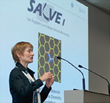
However, for the first time, the recent paper by Jannik C. Meyer et al. [1] demonstrate by a combination of HRTEM experiments and first-principles electronic structure calculations that adjustments to the atomic potentials due to chemical bonding can be discerned in HRTEM images. By comparison of Independent Atom Model (IAM) and Density Functional Theory (DFT) this effect could be calculated, and compared to experimental results of transmission electron microscopy operated in HR-TEM mode. The analyses have been performed for boron nitride (BN) and nitrogen-doped (N-doped) graphene, two sample systems with high scientific and technological interest [7, 8, 9] on a highly promising avenue of 2D materials research. Ute A. Kaiser, director of the German major project SALVE I-II, Ulm University and co-author of the recent paper [1] explained in her celebration talk at the "Green Light for SALVE II" project meeting (see Fig. 1): "Two dimensional materials as graphene and white graphene (BN) are ideal model systems for demonstrating the principal effect of the charge redistribution in an aberration-corrected high-resolution transmission electron microscope (AC-HR-TEM) image, because the thickness is well defined to the one-atom level and no contamination layers on top or underneath the material hamper the investigation. The controlled synthesis of two-dimensional materials with atom substitutions may allow their application as carrier-material for molecules in low voltage aberration corrected high-resolution transmission electron microscopy (LV-AC-TEM)." Understanding the contrast of 2D substrates is a prerequisite in SALVE II where image contrast needs to be assigned to either molecules or substrates.
More Informations: See the citations and comments from other scientists about Meyer et al. 2011 [1] on our website in section "publications" on page "20-80 kV - publications by SALVE authors" and click 'Cited by' behind the reference.
Meyer, J. C., S. Kurasch, H. J. Park, V. Skakalova, D. Künzel, A. Groß, A. Chuvilin, G. Algara-Siller, S. Roth, T. Iwasaki, U. Starke, J. Smet, and U. Kaiser (2011), Experimental analysis of charge redistribution due to chemical bonding by high-resolution transmission electron microscopy. Nature Materials, 10: 209–215, doi: 10.1038/nmat2941, PDF
-
Ruska, E. , M. Knoll (1931), Die magnetische Sammelspule für schnelle Elektronenstrahlen. Z. techn. Physik., 12: 389-400, and 448
-
Knoll, M. , E. Ruska (1932), Das Elektronenmikroskop. Zeitschrift für Physik, 78: 318-339
-
Nobelprize.org, The Nobel Prize in Physics 1986: Ernst Ruska, Gerd Binnig, Heinrich Rohrer
-
The first high-resolution aberration-corrected TEM, equipped with a hexapole corrector [5a], was shown 16 years ago [5b], images were shown 13 years ago [5c-5e] — recently, the initiators received the Wolf-prize in physics for their work [5f] — for more details see Harald Rose’s comprehensive book on electron optics [5g] or current contributions on the history of aberration correction [5h, 5i] and workshops (e. g. [5j]).
-
Rose, H. H. (1990), Outline of a spherically corrected semiaplanatic medium-voltage transmission electron-microscope. Optik, 85: 19
-
Haider, M., G. Braunshausen, E. Schwan. (1995), Correction of the spherical aberration of a 200 kV TEM by means of a hexapole-corrector. Optik, 99: 167–179
-
Haider, M., H. Rose, S. Uhlemann, E. Schwan, B. Kabius, and K. Urban (1998), A spherical-aberration-corrected 200 kV transmission electron microscope. Ultramicroscopy, 74: 53-60, doi: 10.1016/S0304-3991(98)00048-5
-
Haider, M., H. Rose, S. Uhlemann, B. Kabius, and K. Urban (1998), Towards 0.1 nm resolution with the first spherically corrected transmission electron microscope. J. Electron. Microsc., 47: 395-405
-
Haider, M., S. Uhlemann, E. Schwan, H. Rose, B. Kabius, and K. Urban (1998), Electron microscopy image enhanced. Nature, 392: 768, doi: 10.1038/33823
-
Wolf-Award for Breakthrough in Electron Microscopy: Maximilian Haider, Harald Rose, Knut Urban. (2011), News Archive of Microscopy & Microanalysis
-
Rose, H. H. (2009), Geometrical Charged Particle Optics. Springer, Heidelberg
-
Rose, H. H. (2008), History of direct aberration correction. Advances in Imaging and Electron Physics, 156: 1-36, doi: 10.1016/S1076-5670(08)01001-X
-
Rose, H. H. (2009), Historical aspects of aberration correction. J. Electron Microsc., 58: 77-85, doi: 10.1093/jmicro/dfp012
-
Rose, H. H. , M. O'Keefe, A. Lupini, E. Voekl (2011), Theory and techniques of aberration-corrected microscopy. Microscopy and Microanalysis 2011, August, 7-11, Nashville Tennessee
-
-
Binning, G. , H. Rohrer, C. Gerber, und E. Weibel (1982), Surface Studies by Scanning Tunneling Microscopy. Phys. Rev. Lett., 49: 57-61, doi: 10.1103/PhysRevLett.49.57
-
Geim, A. K. (2009), Graphene: status and prospects. Science, 324: 1530-1534, doi: 10.1126/science.1158877
-
Meyer, J. C. , A. Chuvilin, U. A. Kaiser (2009), Graphene – Two-dimensional carbon at atomic resolution. MC2009, 3: 347-348, doi: 10.3217/978-3-85125-6-546
-
Wang, Y., Y. Shao, D. W. Matson, Y. Li, (2010), N-doped graphene and its application in electrochemical biosensing. ACS Nano, 4: 1790-1798, doi: 10.1021/nn100315s


 Download the print version.