First observation of boron nitride chains using low-voltage AC-(S)TEM
December 01, 2014 - A research team from Finland, Japan and Germany under the direction of Arkady V. Krasheninnikov, Kazu Suenaga and Ute A. Kaiser has for the first time created and observed hexagonal boron nitride chains [1]. The researchers find that this new BN-allotrope is stable and that the stability of the chains can be further improved when they are supported by another boron nitride layer. This study completes the family of boron nitride polymorphs with the analogy to carbon, e.g. 2D-BN vs graphene, benzene vs borazine, and fullerenes vs fulborenes [2, 3].

The authors used aberration-corrected low-voltage scanning and high-resolution transmission electron microscopes (LV-AC-(S)TEM) for the irradiation and imaging of the starting 2D-material h-BN. The low voltage limited the damage to the material so that its transformation under the electron-beam could be observed with sub-nanometer resolution in real time.
To interpret the observations, the authors use Molecular Dynamics (MD) simulation and total energy calculation for different possible structures, for example, BN, B, and N-chains and corresponding nanoribbons with a width of one hexagon (Fig. 1 left). It was found, as expected [4] that N-chains are under the prevailing pressure and temperature conditions unstable. For isolated one-hexagon-wide BN nanoribbons the simulations indicated that they transform into two BN chains as a result of the balance between bond formation energy and bending energy. This is in agreement with calculations for one-hexagon-wide carbon nanoribbons, where the same effect has been predicted [5]. The authors also found by simulation, that triangular structures of pure boron, as shown in Fig. 1c, are instable and disintegrate into individual boron chains [6].

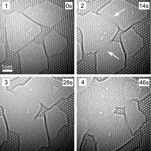
By calculating the temperature-corrected scattering cross section in the electron microscope (Fig. 1 right), the authors find that BN-chains are more stable under electron irradiation than pure B-chains. The calculations revealed that for the generation of knock-on displacement in pristine h-BN, an acceleration voltage of at least 80 kV is required but this value decreases at the edges of large holes for B-atoms to 40 kV and for N-atoms to 60 kV. However, in the experiment it was found that defects also occur below the calculated limits. An example is shown in Fig. 2, single-layer h-BN is progressively damaged although acceleration voltages as low as 15 kV and 30 kV were used - and the growth rate of holes at 15 kV is even higher than at 30 kV.
Ute Kaiser, leader of the group Electron Microscopy of Materials Science (EMMS) at Ulm University, said: "We have observed this effect already in studies of graphene with 20 keV electrons. [7]. The damage below the knock-on threshold is probably formed by chemical reactions between the sample and the residuals in the microscope vacuum (high vacuum). To further avoid radiation damage, an ideal solution would be on the one hand to use acceleration voltages below the knock-on threshold (to prevent direct removal of atoms, but still allow sufficient resolution), and on the other hand, to achieve better vacuum (ultra-high vacuum) in the electron microscope to limit the effects of chemical etching."
Determining mechanical and electrical properties

If B and N atoms are removed from the edges, either by knock-on collision or by chemical etching, the width of the BN nanoribbons reduces progressively until a thickness of 1 hexagon is obtained, wherein the structures become unstable and decay into two BN chains. At 80 kV this mechanism precludes the formation of pure B-structures (Fig. 3) because B atoms are preferential targets for sputtering. The cross sections shown in Figure 1 demonstrate that B-ribbons and chains are unstable under these imaging conditions (Fig. 1).
By using the formula of [8], the team now showed that the lifetime of BN chains is influenced by the supporting substrate. In the case of BN-chains on a h-BN substrate, the simulation results consistent with the experiments indicated lifetimes in the range of several 10 min [9]. In contrast, suspended BN chains have a significantly lower lifetime, despite the lower acceleration voltage used in the experiment. A possible cause of breaking that was also considered is strain. Calculations predict a tolerable value of 7%, which is lower than the general calculated results for carbon chains [10, 5]. Strain is caused by the degradation of the BN layer on both ends of the BN chain. Another significant cause could be vibration. However, these two causes of instability are far less important in supported BN-chains because the underlying h-BN layer gives them freedom to adapt by changing the anchor point at surface defects or at other points on the edges of the shrinking layer (Fig 3). Another reason, the authors note, could be change in the chain structure and bonding through diffusing atoms on the surface of the substrate.
The authors point out further analogies to the structural analogues of BN-chains. Carbon chains were also made of few-layer graphene and observed in the TEM [11]. A common problem is the absence of structural information about the chain itself, even in cases where the resolution and the signal-to-noise ratio should make the observation possible. This has been explained by the vibration of the chains. Recent calculations show that the strain in carbon chains increases with increasing strain [12]. When compared to graphene these chains are very poor conductors with a band gap that also increases with strain [11, 12]. This is in agreement with the calculations of the authors that predict that BN chains are insulating. In addition to demonstrating that the electron beam can produce and image this previously unobserved 1D-material, the author highlight that BN-chains could be used to interconnect two-dimensional materials in semiconductor devices [13].
-
Cretu, O., Komsa, H. P., Lehtinen, O., Algara-Siller, G., Kaiser, U., Suenaga, K., & Krasheninnikov, A. V. (2014). Experimental Observation of Boron Nitride Chains. ACS nano 8: 11950-11957, doi: 10.1021/nn5046147
-
Kroto, H. W., Heath, J. R., O'Brien, S. C., Curl, R. F., Smalley, R. E. (1985) C60: Buckminsterfullerene. Nature 1985: 162–163, doi: 10.1038/318162a0
-
Golberg, D., Bando, Y., Stéphan, O., & Kurashima, K. (1998). Octahedral boron nitride fullerenes formed by electron beam irradiation. Applied Physics Letters 73: 2441-2443, doi: +10.1063/1.122475
-
Buchsbaum, S., Mills, R. L., & Schiferl, D. (1984). Phase diagram of nitrogen determined by Raman spectroscopy from 15 to 300 K at pressures to 52 GPa. The Journal of Physical Chemistry 88: 2522-2525, doi: 10.1021/j150656a018
-
Liu, M., Artyukhov, V. I., Lee, H., Xu, F., & Yakobson, B. I. (2013). Carbyne from first principles: chain of C atoms, a nanorod or a nanorope. ACS nano 7: 10075-10082, doi: 10.1021/nn404177r
-
Boustani, I. (1997). Systematic ab initio investigation of bare boron clusters: Determination of the geometry and electronic structures of Bn (n=2–14). Physical Review B 55: 16426, doi: 10.1103/PhysRevB.55.16426
-
Meyer, J. C., Eder, F., Kurasch, S., Skakalova, V., Kotakoski, J., Park, H. J., Roth, S., Chuvilin, A., Eyhusen, S., Benner, G., Krasheninnikov, A. V., & Kaiser, U. (2012). Accurate measurement of electron beam induced displacement cross sections for single-layer graphene. Physical Review Letters 108: 196102, doi: 10.1103/PhysRevLett.108.196102
-
Banhart, F. (1999). Irradiation effects in carbon nanostructures. Reports on Progress in Physics 62: 1181, doi: 10.1088/0034-4885/62/8/201
-
Kotakoski, J., Jin, C. H., Lehtinen, O., Suenaga, K., & Krasheninnikov, A. V. (2010). Electron knock-on damage in hexagonal boron nitride monolayers. Physical Review B 82: 113404, doi: 10.1103/PhysRevB.82.113404
-
Nair, A. K., Cranford, S. W., & Buehler, M. J. (2011). The minimal nanowire: Mechanical properties of carbyne. EPL 95: 16002, doi: 10.1209/0295-5075/95/16002
-
Cretu, O., Botello-Mendez, A. R., Janowska, I., Pham-Huu, C., Charlier, J. C., & Banhart, F. (2013). Electrical transport measured in atomic carbon chains. Nano letters 13: 3487-3493, doi: 10.1021/nl4018918
-
Artyukhov, V. I., Liu, M., & Yakobson, B. I. (2013). Mechanically induced metal-insulator transition in carbyne. Nano Letters 14: 4224-4229, doi: 10.1021/nl5017317
-
Rong, Y., & Warner, J. H. (2014). Wired Up: Interconnecting Two-Dimensional Materials with One-Dimensional Atomic Chains. ACS nano In press, doi: 10.1021/nn5065524