2D-materials in supersaturation: First observation of implanted self-interstitials enabled by LV-AC-HRTEM
January 14, 2015 - In the new issue of Nano Letters researcher report for the first time that they have succeeded to image implanted self-interstitials at the example of the material graphene [1]. The scientists from the group of Electron Microscopy of Materials Science at the University of Ulm with the principle investigator Ossi Lehtinen succeeded in producing self-interstitials by the use of a simple carbon coating device, normally used for the deposition of conductive amorphous carbon films on non-conducting samples for imaging in the electron microscope. By using low-voltage aberration-corrected high-resolution transmission electron microscopy (LV-AC-HRTEM) at an accelerating voltage of 80 kV they were able to demonstrate all previously theoretically predicted structures [2] experimentally and, in addition, also larger aggregates.
Challenges in creation and imaging of implanted self-interstitials
The introduction of the 2-dimensional crystals in the zoo of known materials enabled a totally new perspective for the study of defects. This is mainly due to the simple reason that the three-dimensional nature of the solids does not obscure the view of the defects in the case of 2D materials, because the surface is all that these 2D materials have. As a consequence, this new class of materials has supported the studies of defects, such as defects produced by ion [3] or electron beam radiation [4], grain boundaries [5], dislocations [6,7] and impurity atoms that replace material atoms or which are adsorbed on the material [8]. However, the imaging of implanted self-interstitials at atomic resolution had until now neither been achieved for a 3-dimensional, nor for a 2-dimensional material.
Beside low-voltage aberration-corrected scanning transmission electron microscopy (LV-AC-STEM) and scanning tunneling microscopy (STM) LV-AC-HRTEM belongs to the modern methods by which the exact atomic structure of 2D materials can be mapped [9]. The experimental detection of a single carbon adatom, which is situated on a sp2 C-C bond, had already been achieved [10]. Dimers had also already been detected in hexagonal 2D silicon oxide monolayers [11,12], and in graphene [12,13] in previous studies, but these structures were either created by incomplete crystallization, or by exposure to extremely high electron doses in a TEM. Hereafter, a large number of atoms was removed around the defect and the entire lattice was rearranging, which in addition produced numerous other defects. The imaging of isolated self-interstitial dimers without defects in their vicinity or of a crystal in a state of super-saturation, which leads to the formation of self-interstitials, could not be achieved so far, despite extensive studies on the atomic scale.
There are several reasons, which have prevented this observation so far. The preparation of simple defects in graphene can be easily achieved in the TEM by exposing the material to the electron beam of the microscope, since an accelerating voltage of 80 kV and above is sufficient to remove an atom from the crystal by individual knock-on collision between an electron and a carbon atom in graphene. However, new carbon atoms must be available for the introduction of an additional atom. What furthermore complicates the generation of an adatom in the TEM is the fact that on the one hand, the electron beam can remove this atom by knock-on and the displacement threshold energy of an atom of such a defect site tends to be even lower than for pristine graphene [14]. On the other hand, it is energetically consuming to achieve a positive density change in a crystal.


Electron-beam-mediated rearranging of supersaturated graphene
Here the researchers could take advantage of a positive feature of graphene. As it can be deformed in the direction outside the plane of the atoms and due to the low bending modulus [15], the energy required for the introduction of an additional atom is relatively low. To estimate the parameters required for the production of self-interstitials in graphene, the authors performed molecular dynamics (MD) simulations. Their results, which are supported by previous calculations of the binding energies of these defects [16] show that the electron beam in the microscope can provide the energy to the system to allow the atoms to overcome the activation barrier, without causing knock-on damage.

From an analysis of the TEM images, immobile adsorbants like e.g. CH3 molecules [16] can easily be identified, however the identification of single C-adatoms on graphene is rather unlikely, since these are mobile at room temperature [2]. However, the identification of self-interstitial dimers on the TEM images is easily possible. For these defects, it is predicted that they are integrated into the sp2-bonded graphene lattice without dangling bonds [2]. Polygon pattern consisting of pentagons, hexagons and heptagons, are clearly visible (see Fig. 1), especially if an aberration of the electron lens, the A2 astigmatism, is corrected by filtering (Fig. 2).
After inclusion of additional carbon atoms it is mostly even physically impossible to determine which exactly the newly added atoms are. The structures become identical either to the so-called Stone-Thrower-Wales type defects (Fig. 1a) [2], or to larger structures, which can consist of miniscule grain boundary loops with associated density surplus [17], as for example in case of the dimers in Fig. 1b and c, where a chain of pentagons and heptagons encloses one or two hexagons.
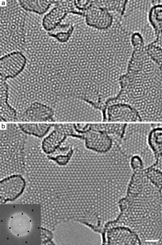
A limit to the producible density of interstitials in the graphene layer is achieved when the deposited layer thickness is increased to about one monolayer. Instead of being integrated in the graphene grid, the additional carbon atoms segregate to a new layer. High resolution images show the formation of a new nanocrystalline graphene layer (Fig. 3a). If the contribution of the first graphene layer to the image is removed by Fourier filtering, nanometer-wide graphene grains are visible, which are separated by chains of pentagonal and heptagonal carbon rings (Fig. 3b).
However, by careful adjustment of the deposition parameters, a sufficiently low density of extra carbon can be achieved in order to produce isolated point defects. For all interstitial structures a strong bulge outside the atom plane is expected. The researchers note, that those bubble-like structures have higher reactivity than pure graphene, which may be advantageous for further functionalization. Furthermore, the surplus atoms can have highly interesting electronic and magnetic properties [2]. In addition to the demonstration of how the previously impossible imaging of implanted self-interstitials can be achieved and thus to contribute to the fundamental understanding of crystallographic defects, the findings offer new routes for the creation of custom graphene-based and other 2D materials, because the self-interstitials can be used to specifically functionalize the materials by placing the crystals in a metastable state of supersaturation.
Highlighted Topics
Why crystal defects play a key role in determining the material properties
-
Lehtinen, O., Vats, N., Algara-Siller, G., Knyrim, P., & Kaiser, U. (2014). Implantation and atomic scale investigation of self-interstitials in graphene. Nano letters 15: 235–241, doi: 10.1021/nl503453u
-
Lusk, M. T., Wu, D. T., & Carr, L. D. (2010). Graphene nanoengineering and the inverse Stone-Thrower-Wales defect. Physical Review B 81: 155444, doi: 10.1103/PhysRevB.81.155444
-
Standop, S., Lehtinen, O., Herbig, C., Lewes-Malandrakis, G., Craes, F., Kotakoski, J., Michely, T., Krasheninnikov, A. V., & Busse, C. (2013). Ion impacts on graphene/Ir (111): interface channeling, vacancy funnels, and a nanomesh. Nano letters 13: 1948-1955, doi: 10.1021/nl304659n
-
Meyer, J. C., Eder, F., Kurasch, S., Skakalova, V., Kotakoski, J., Park, H. J., Roth, S., Chuvilin, A., Eyhusen, S., Benner, G., Krasheninnikov, A. V., & Kaiser, U. (2012). Accurate measurement of electron beam induced displacement cross sections for single-layer graphene. Physical Review Letters 108: 196102, doi: 10.1103/PhysRevLett.108.196102
-
Yazyev, O. V., & Louie, S. G. (2010). Topological defects in graphene: Dislocations and grain boundaries. Physical Review B 81: 195420, doi: 10.1103/PhysRevB.81.195420
-
Warner, J. H., Margine, E. R., Mukai, M., Robertson, A. W., Giustino, F., & Kirkland, A. I. (2012). Dislocation-driven deformations in graphene. Science 337: 209-212, doi: 10.1126/science.1217529
-
Lehtinen, O., Kurasch, S., Krasheninnikov, A. V., & Kaiser, U. (2013). Atomic scale study of the life cycle of a dislocation in graphene from birth to annihilation. Nature communications 4, doi: 10.1038/ncomms3098
-
Bangert, U., Pierce, W., Kepaptsoglou, D. M., Ramasse, Q., Zan, R., Gass, M. H., Van den Berg, J. A., Boothroyd, C. B., Amani, J., & Hofsäss, H. (2013). Ion Implantation of Graphene - Toward IC Compatible Technologies. Nano letters 13: 4902-4907, doi: 10.1021/nl402812y
-
Coraux, J., Plasa, T. N., Busse, C., & Michely, T. (2008). Structure of epitaxial graphene on Ir (111). New Journal of Physics 10: 043033, doi: 10.1088/1367-2630/10/4/043033
-
Girit, Ç. Ö., Meyer, J. C., Erni, R., Rossell, M. D., Kisielowski, C., Yang, L., Park, C. H., Crommie, M. F., Cohen, M. L., Louie, S. G., & Zettl, A. (2009). Graphene at the edge: stability and dynamics. Science 323: 1705-1708, doi: 10.1126/science.1166999
-
Yu, X., Yang, B., Boscoboinik, J. A., Shaikhutdinov, S., & Freund, H. J. (2012). Support effects on the atomic structure of ultrathin silica films on metals. Applied Physics Letters 100: 151608, doi: 10.1063/1.3703609
-
Björkman, T., Kurasch, S., Lehtinen, O., Kotakoski, J., Yazyev, O. V., Srivastava, A., Skakalova, V., Smet, J. H., Kaiser, U., & Krasheninnikov, A. V. (2013). Defects in bilayer silica and graphene: common trends in diverse hexagonal two-dimensional systems. Scientific reports 3, doi: 10.1038/srep03482
-
Robertson, A. W., He, K., Kirkland, A. I., & Warner, J. H. (2014). Inflating graphene with atomic scale blisters. Nano letters 14: 908-914, doi: 10.1021/nl404266k
-
Susi, T., Kotakoski, J., Arenal, R., Kurasch, S., Jiang, H., Skakalova, V., Stephan, O., Krasheninnikov, A. V., Kauppinen, E. I., Kaiser, U. A., & Meyer, J. C. (2012). Atomistic description of electron beam damage in nitrogen-doped graphene and single-walled carbon nanotubes. ACS nano 6: 8837-8846, doi: 10.1021/nn303944f
-
Yakobson, B. I., Brabec, C. J., & Bernholc, J. (1996). Nanomechanics of carbon tubes: instabilities beyond linear response. Physical review letters 76: 2511, doi: 10.1103/PhysRevLett.76.2511
-
Lee, Z., Jeon, K. J., Dato, A., Erni, R., Richardson, T. J., Frenklach, M., & Radmilovic, V. (2009). Direct Imaging of Soft− Hard Interfaces Enabled by Graphene. Nano letters 9: 3365-3369, doi: 10.1021/nl901664k
-
Cockayne, E., Rutter, G. M., Guisinger, N. P., Crain, J. N., First, P. N., & Stroscio, J. A. (2011). Grain boundary loops in graphene. Physical Review B 83: 195425, doi: 10.1103/PhysRevB.83.195425