Electron beam induced formation and evolution of defects in monolayer WSe2
September 22, 2020 - Transition metal dichalcogenide (TMD) monolayers have attracted significant interest due to their direct bandgap, which may be influenced by lattice defects. Scientists from the group of electron microscopy for materials science at Ulm university have studied the electron-beam-induced defect dynamics in monolayer WSe2 by atomically resolved in-situ transmission electron microscopy.
After the discovery of graphene, two-dimensional transition metal dichalcogenides (2D-TMDs) have received increasing attention. Similar to graphite, layers are bound by van-der-Waals bonds, and TMD monolayers can be exfoliated with the scotch tape [1]. Extraordinary mechanical, electrical, magnetic and optical properties are reported for 2D-TMDs [2, 3]. Among numerous members of the class of 2D-TMDs, tungsten diselenide (WSe2) are considered a very promising candidate with a wide range of optoelectronic applications [4–8]. For instance, it opens its direct bandgap from 1.2 eV in bulk [9] to 1.7 eV in the monolayer structure [10].
The formation of lattice defects can modify the properties of TMD monolayers in addition. For example, point defects are shown to create localized excitons in monolayer WSe2 [11]. These states can not only arise from the growth process of the crystal [12] but can also be created afterwards, for example, by electron irradiation via several mechanisms of transferring energy from the impinging electrons to the lattice [13, 14]; those pathways can in principle be followed atom-by-atom if the resolution of the transmission electron microscope (TEM) is sufficient.
Scientists have now studied the defect formation and evolution in monolayer WSe2 at atomic resolution in the TEM. Due to the lower atomic number of Se compared to W, Se atoms are more prone to be ejected from the WSe2 lattice by electron irradiation, which results in the formation of single Se vacancies as well as double Se vacancy columns [15]. By utilizing an electron beam of variable energy, one can even create particular defects. This can, potentially, also be used to tailor unique properties in 2D-TMD materials [17]. It has already been reported that with increased total electron dose, more and more complex defect structures form [18]. Some of these defects agglomerate to line-shaped structures, so called line defects [19, 20], which affect the electronic structure and in some cases even add magnetic moments [21]. The orientation of the line defects can be controlled by directional strain on the material [19]. Mirror twin boundaries (MTBs) are one type of these line defects which have been intensively studied recently [21, 23, 24]. One of the reasons for the interest in MTBs is the change of the material properties they cause. Lin et al. [16] had recently shown that MTBs give rise to p-type doping and local magnetic moments in WSe2. Thus far, three different types of MTBs have been observed in TMDs, commonly denoted as 4|4P, 4|4E and 55 × 8 [26]. In the case of WSe2, only the 55 × 8 type had been observed at high temperatures of 500 °C [16].
In their new study, the researchers used low accelerating voltages of the electron microscope. At medium electron accelerating voltages of 200–300 kV, electron-beam-sensitive 2D materials are often fast destroyed during imaging due to knock-on collusions between the electrons and the atoms. Decreasing knock-on damage while maintaining atomic resolution has been the driving force behind decreasing the voltage, at which the TEM operates down to 20–80 kV and corrects not only the CS but also the chromatic aberration (CC) of the objective lens for higher resolution [27]. The CS- and CC-corrected SALVE TEM is especially useful to study the dynamics of 2D materials at lower accelerating voltages in high-resolution TEM (HRTEM) mode, as it allows, in contrast to the STEM mode, to track the structural rearrangements atom-by-atom in real time [28], while maintaining a large field of view in a single exposure and collecting the information from all scattered electrons.
Thus, the scientists now report the formation and evolution of defects in monolayer WSe2 at room temperature, including all three types of MTBs as well as a fourth type, which was not observed in TMDs so far. They also report on the evolution of the defects with continued electron irradiation from single Se vacancies over extended defects to the rupture of the monolayer.
Initial radiation damage
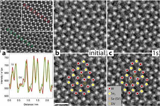
After accumulating a higher electron dose of 1.0 × 10⁸ e-/nm2 on the specimen [29], which is about a factor of 1000 higher compared to the initial image, they observed the formation of single Se vacancies which tend to transfer into double Se vacancy columns (Figure 1a). Here they inserted in the right upper corner a simulated image with one double Se vacancy column and one single Se vacancy, using the experimental parameters as described in the method section. One can identify the positions of W and Se and distinguish double Se vacancy columns from single Se vacancies (see the agreement between the red (calculation) and green (experiment) line profiles through single Se vacancy and double Se vacancy column). By comparing subsequent images of the image series, they observe a high mobility of double Se vacancy columns, resulting in back and forth jumping of double Se vacancy columns as exemplified in Figures 1b,c. This can be explained by the low energy barrier for migration in WSe2, as was already reported in literature [22, 30].
Formation of complex extended structures
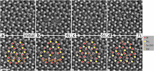
As Se atoms continue to be ejected under further electron irradiation, more complex extended defect structures evolve. Figure 2 shows the formation of a symmetric trefoil defect, which requires a deficit of six Se atoms; in the lower raw of the images the same images are displayed together with the marked atoms for better understanding of the defect formation process. We identify the formation path as a multi-step process, which also includes asymmetric rings as follows: In Figure 2a two double vacancies form, as well as five single vacancies as shown schematically in the lower image. The atoms then rearrange (see Figure 2b) to fill up the voids in the upper part of the structure, while creating two irregularly shaped rings and a staggered double vacancy line again schematically shown in the lower image of Figure 2b). In the next step, the atoms rearrange into one 8-membered ring as marked in the lower image (Figure 2c). Finally, two more rings are formed by a simple move of one Se2 column down and two W atoms up. This is in contrast to previously suggested formation pathways, requiring a specific triangular arrangement of double vacancies and a subsequent bond rotation [16]. This discrepancy may be associated to the local distribution of missing atoms and therefore may not follow the energetically lowest pathway.
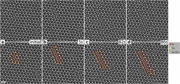
As more and more Se atoms are removed from the lattice they observe line defects consisting of multiple Se vacancies. Figure 3 shows the formation of a 2.3 nm long double Se vacancy line with 15 lost Se atoms. The growth process is driven now by the collapse of hexagons, which contain three single Se vacancies shown in Figure 3a. In this step, the remaining single Se atoms move inward of the former hexagon. This process continues as more vacancies are created by the electron beam. It is conceivable that this process and the direction of the line growth depends on lattice strain, which is induced by the rigidity of the holey carbon grid supporting the monolayer. Such preferential orientation was previously reported for MoS2 by Komsa et al [19]. Curiously, the growth of the defect pauses for over 1 min or 5.1 × 10⁷ e-/nm2 in between Figures 3b,c, before another interval of rapid growth sets in Figures 3c,d.
In the timeframe after the formation of one-dimensional defects (line defects), they began to observe extended two-dimensional defects. One type of these structures forms as inversion domains, which are terminated with MTBs. An example of such a formation process is shown in Figure 4. We observe that in this case, two staggered double vacancy lines glide into each other and recombine by moving the lower Se atoms on top of the ones to the upper right of their respective positions while the W atoms move down and to the left. This in turn causes a glide of the Se planes against the W plane, were the Se2 columns move down and the W atoms move up within the triangular area seen in Figure 4. In this case, the MTBs, which terminate the inversion domain on the left in Figure 4a are all 4|4P structures. Such a termination has been previously reported for MoS2 and MoSe2, but not in WSe2 [22, 23, 25].
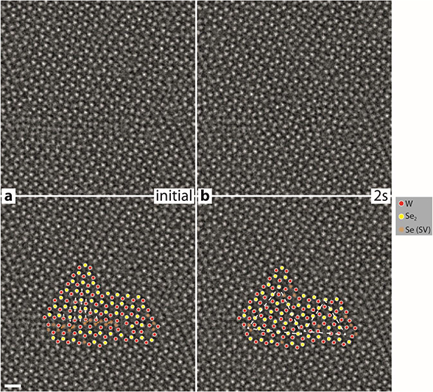
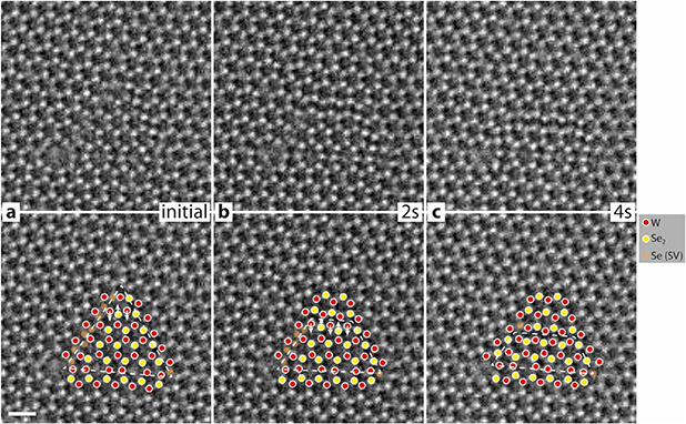
With increased accumulated electron dose, they observed further structural changes for inversion domains and MTBs. In Figure 5a they observed an inversion domain with all three types of MTBs known in TMDs so far, including not only the 4|4P type on the right, as mentioned above, 55 × 8 at the bottom, but in addition the 4|4E MTB, which also was not found in previous reports on WSe2. 2 s later, they observed the inversion domain to shrink from the top, simultaneously the Se atoms move up and the W atoms move down, resulting in two W planes without Se atoms between. This is a new type of MTB, which appears at the top of the trapezium domain. This MTB has similar edge type symmetry to the 4|4E structure, but without the staggered single Se atoms in the center. We therefore denote this new type of MTB as 4|4E'. In addition to the shrinkage of the inversion domain and further gliding of the new type of MTB, they observed a change in the left side of the inversion domain, where the MTB changes from 4|4E to 4|4P. We suggest that this evolution of the inversion domain is caused by changes to the strain state of the surrounding lattice. We speculate, that this could lead to the original domain structure being energetically favorable again, similar to the report of Komsa et al. [19].
Formation of holes
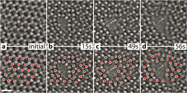
As the scientists continued to irradiate the sample, the increasingly strained lattice leads to the formation of holes in the film. Despite this, the W atoms are not sputtered until the local ratio between W and Se approaches 1:1 (Figure 6). In Figure 6a, they saw the initial state with an already slightly defective, but still continuous layer. As more Se atoms are ejected, a hole starts to form (Figure 6b). However, the number of W atoms, marked in red, remains the same. This also holds for panel (c), where the size of the hole is extended further as more Se atoms are removed. The W atom marked by the white arrow is the first one, which is removed in Figure 6d. As this occurs, the number of Se atoms has been reduced to about the same as the W atoms. Recently, Zhao et al. demonstrated the formation of a pure Mo islands within MoS2 [31]. However, their STEM irradiated only a small area on the sample at the same time, keeping the unirradiated area still stoichiometric without defects. In this case, a much larger area was under irradiation. The area was full of defects with loss of many Se atoms at this stage. The strained, almost destroyed monolayer is not compatible with an active pure W cluster. This could explain why they did not observe analogous behavior in the experiments.
"We have shown atom-by-atom electron-beam-induced and electron-dose-dependent formation and evolution of different defect types in monolayer WSe2 from initial point defects to extended holes. In particular, they could study the evolution of point defects over line defects, more extended defects to 2D defect structures taking also unusual pathways. We found that the evolution is more complex than suggested from theoretical calculations.", Ute Kaiser, lead author of the sudy, said. "Previously unreported MTBs were formed and it was shown how they developed dynamically with increasing electron dose."
The newly discovered boundaries are of particular interest with respect to modification of the electronic properties of the material. With further increased electron dose, highly defective W-rich regions within the WSe2 matrix formed, paving ways towards future device engineering. In general, the study may help to tailor devices composed of defined defect controlled WSe2 monolayers with specific electronic and magnetic properties in the future.
Resource: Leiter, R., Li, Y., & Kaiser, U. (2020). In-situ formation and evolution of atomic defects in monolayer WSe2 under electron irradiation. Nanotechnology, 31(49), 495704
-
Novoselov, K. S. et al. Two-dimensional atomic crystals. Proc. Natl Acad. Sci. 2005 102 10451–10453.
-
Wang Q. H. et al. Electronics and optoelectronics of two-dimensional transition metal dichalcogenides. Nat. Nanotechnol. 2012 7 699–712.
-
Chhowalla M. et al. The chemistry of two-dimensional layered transition metal dichalcogenide nanosheets. Nat. Chem. 2013 5 263–75.
-
Radisavljevic B. et al. Single-layer MoS2 transistors. Nat. Nanotechnol. 2011 6 147–50.
-
Cheng Q. et al. WSe2 2D p-type semiconductor-based electronic devices for information technology: design, preparation, and applications. InfoMat 2020 2 656–97.
-
De Luca M. et al. New insights in the lattice dynamics of monolayers, bilayers, and trilayers of WSe2 and unambiguous determination of few-layer-flakes’ thickness. 2D Mater. 2020 7 025004.
-
Smyth C. M. et al. Engineering the interface chemistry for scandium electron contacts in WSe2 transistors and diodes. 2D Mater. 2019 6 045020.
-
Król M. et al. Exciton-polaritons in multilayer WSe2 in a planar microcavity. 2D Mater. 2019 7 015006.
-
Kam K. K. and Parkinson B. A. Detailed photocurrent spectroscopy of the semiconducting group VIB transition metal dichalcogenides. J. Phys. Chem. 1982 86 463–7.
-
Ding Y. et al. First principles study of structural, vibrational and electronic properties of graphene-like MX2 (M=Mo, Nb, W, Ta; X=S, Se, Te) monolayers. Phys. B Condens. Matter 2011 406 2254–60.
-
Zhang S. et al. Defect structure of localized excitons in a WSe2 monolayer. Phys. Rev. Lett. 2017 119 046101.
-
Mortelmans W. et al. Fundamental limitation of van der Waals homoepitaxy by stacking fault formation in WSe2. 2D Mater. 2020 7 025027.
-
Algara-Siller G. et al. The pristine atomic structure of MoS2 monolayer protected from electron radiation damage by graphene. Appl. Phys. Lett. 2013 103 203107.
-
Lehnert T. et al. Electron radiation damage mechanisms in 2D MoSe2. Appl. Phys. Lett. 2017 110 033106.
-
Komsa H.-P. et al. Two-dimensional transition metal dichalcogenides under electron irradiation: defect production and doping. Phys. Rev. Lett. 2012 109 035503.
-
Lin Y.-C. et al. Three-fold rotational defects in two-dimensional transition metal dichalcogenides. Nat. Commun. 2015 6 6736.
-
Komsa H.-P. et al. Engineering the electronic properties of two-dimensional transition metal dichalcogenides by introducing mirror twin boundaries. Adv. Electron. Mater. 2017 3 1600468.
-
Ryu G. H. et al. Atomic structure and dynamics of self-limiting sub-nanometer pores in monolayer WS2. ACS Nano 2018 12 11638–47.
-
Komsa H.-P. et al. From point to extended defects in two-dimensional MoS2: evolution of atomic structure under electron irradiation. Phys. Rev. B 2013 88 035301.
-
Chen Q. et al. Ultralong 1D vacancy channels for rapid atomic migration during 2D void formation in monolayer MoS2. ACS Nano 2018 12 7721–30.
-
Lehnert T. et al. Electron-beam-driven structure evolution of single-layer MoTe2 for quantum devices. ACS Appl. Nano Mater. 2018 2 3262–70.
-
Lin J. et al. Vacancy-induced formation and growth of inversion domains in transition-metal dichalcogenide monolayer. ACS Nano 2015 9 5189–97.
-
Lehtinen O. et al. Atomic scale microstructure and properties of Se-deficient two-dimensional MoSe2. ACS Nano 2015 9 3274–83.
-
Diaz H. C. et al. High density of (pseudo) periodic twin-grain boundaries in molecular beam epitaxy-grown van der Waals heterostructure: moTe2 /MoS2. Appl. Phys. Lett. 2016 108 191606.
-
Wang S. et al. Detailed atomic reconstruction of extended line defects in monolayer MoS2. ACS Nano 2016 10 5419–30.
-
Zhou W. et al. Intrinsic structural defects in monolayer molybdenum disulfide. Nano Lett. 2013 13 2615–22.
-
Linck M. et al. Chromatic aberration correction for atomic resolution TEM imaging from 20 to 80 kV. Phys. Rev. Lett. 2016 117 076101.
-
Huang P. Y. et al. Imaging atomic rearrangements in two-dimensional silica glass: watching silica’s dance. Science 2013 342 224-227.
-
Zhao X. et al. Engineering and modifying two-dimensional materials by electron beams. MRS Bull. 2017 42 667–676.
-
Lin J. et al. Flexible metallic nanowires with self-adaptive contacts to semiconducting transition-metal dichalcogenide monolayers. Nat. Nanotechnol. 2014 9 436–42.
-
Zhao X. et al. Atom-by-atom fabrication of monolayer molybdenum membranes. Adv. Mater. 2018 30 1707281.

