Accurate measurement of knock-on damage in graphene
May 7, 2012 - Radiation damage resulting from the collision of beam electrons with an atomic nucleus (Knock-on damage) is a problem with which electron microscopists must deal every day when imaging sensitive materials. It is generally known that imaging of graphene requires acceleration voltages ≤ 80 kV [1, 2]. In spite of its great importance, a comprehensive quantitative analysis is missing among the studies published so far [3 - 6]. The new study now closes this gap and unravels the underlying physical processes. The first accurate measurement of electron beam induced displacement cross section in single layer graphene can largely be explained theoretically if the lattice vibrations are taken into account, according to a new study carried out at Ulm University in the frame of the SALVE project.

Knock-on damage is an important radiation damage processes in transmission electron microscopy [7]. For this direct removal of an atom after collision with an electron, light materials such as carbon nanotubes [8, 9], fullerenes [10], graphene [11], 12] and boron nitride [13] are particularly vulnerable [3]. In addition, imaging of these materials also necessitates very high electron doses because they produce low contrast and usually contain only one or very few atoms in the projection direction. The continuous improvement of the instrumental resolution [14, 15] further increases the required electron doses in the last years [16]. Furthermore, the need for high doses is increased even further for new techniques such as single-atom or single-atomic-column spectroscopy [16, 17], atomic resolution electron tomography [18], or the analysis of charge distributions from very high signal-to-noise ratio HRTEM images [1].
The new study now provides a comprehensive quantitative analysis of the physical processes underlying knock-on damage [26->19], which goes beyond the analysis in studies published so far [3 - 6, 20]. Here, graphene is used as a test material. It can be prepared in a precisely defined geometry (1 atomic layer thick, hexagonal lattice, with practically no defects), is relatively easy to model, and the number of ejected atoms in multi-vacancy configurations can be directly obtained from HRTEM images [2, 21].
The findings, published in the journal Physical Review Letters, may resolve a longstanding mystery: Why is graphene knock-on damage already occurring at slightly above 80 keV when the binding energy of carbon in graphene corresponds to the energy transferred at 108 keV?
"Knock-on damage occurs, if the amount of energy transferred from an electron to an atom exceeds the binding strength of the lattice," said SALVE scientists Jannik Meyer, lead author of the study. "By considering the lattice vibrations of the material, we were able to show that the experimental results are consistent with the model on the Coulomb interaction between an electron and an atomic nucleus."
Study co-authors include SALVE director Ute Kaiser as well as further scientists from Ulm University, the company Carl Zeiss Microscopy, the Max-Planck-Institute for Solid State Research Stuttgart, as well as the Universities Helsinki und Aalto in Finland and the Korea University in Seoul.
Quantifying knock-on radiation damage
In order to distinguish between radiation damage caused by knock-on and other effects like chemical etching or radiolysis, the scientists used graphene test samples with the natural isotope ratio (98.9% 12C, 1.1% 13C) and "heavy graphene" which consists only of 13C. Graphene with the natural isotope distribution was prepared by exfoliation [22] and chemical vapor deposition (CVD) [23]. Heavy graphene was also produced by the standard CVD process, but the synthesis gas was replaced by 99% 13C enriched methane.
Since the knock-on threshold of carbon in low-dimensional allotropes (CNT, graphene, fullerene) is in the range of > 80 kV [5], measurements were performed at 80, 90, 95 and 100 kV using the aberration-corrected FEI Titan TEM of the University of Ulm. Spherical aberration and focus were set so that the contrast could be directly interpreted as atomic structure. In order to further distinguish radiation damage processes which are depending on acceleration voltage from kV-independent types of radiation damage, additional experiments were carried out at 20 kV with the SALVE II TEM [24], an aberration-corrected Zeiss Libra at Carl Zeiss Microscopy. Time series of 100 images with 1 s exposure time and 2 - 4 s between two successive images were usually recorded. (Video 1)
Video 1. Observation on knock-on damage in graphene by HRTEM
Fig. 1 shows images of 12C graphene taken at 100 kV. The original HRTEM image is shown on the left, the same image superimposed with a structure corresponding to the atomic configuration is shown on the right. In order to count the missing atoms, a frame around was drawn the defective cluster and the number of atoms present was compared with the unchanged material state (see Fig. 1) [21, 2]. The number of defects could be obtained up to an electron energy of 100 kV for 12C, since the formation of defects for energies in that region takes place sufficiently slowly that it can be captured in the time series.

The result of this study is shown in Fig. 2, where the number of missing atoms per area is shown for the different acceleration voltages and isotopes. The study includes the analysis of a tremendous data set (see Supplementary Material for further examples). The slope of the linear fit directly allows the determination of the experimental knock-on cross section. For the 100 kV case, 2 independent measurements were carried out with the dose rates 3.5 × 10⁵ e-/(nm2s) and 1 × 10⁶ e-/(nm2s). From the two nearly identical results, a dose rate effect can be excluded. Under 80 kV irradiation (not shown in Fig. 2), no defects could be detected up to very high doses (above 1010 e-/(nm2s).

Knock-on damage vs. chemical etching
For the new study the scientists were interested in radiation damage due to knock-on collisions of a beam electron and an atomic nucleus. Therefore, they examined radiation damage in the two different materials: 12C and 13C graphene. Comparing the data sets for initially pristine, clean, and defect free graphene, one finds that the generation of defects depends on the acceleration voltage and the isotope composition. Fig. 3 shows two graphene membranes after irradiation with 95 kV, where the difference is most clearly visible. Hence, the process must be the result of a direct collision of a beam electron with a carbon atom core: any chemical effect or ionization would not differ between 12C and 13C.
The removal of atoms also occurs at the outer edges of graphene [25]. To determine whether this effect leading to the growth of extended holes is due to knock-on damage or chemical etching, the effect was studied at different acceleration voltages including 20 kV. Knock-on of edge atoms in graphene should not take place at acceleration voltages below 50 kV [26]. However, the growth of extended holes is also observed at 20 kV (see Fig. 3e and supplemental material). As can be seen in Figs. 3c and 3d, extended holes are always formed in places where contamination is present. The scientists also found that the rate of growth is related to the vacuum level in the TEM that varied in the range of 10-6 to 10-7 mbar. The lower the pressure, the less the growth of extended holes. All these results are agreeing with the expectations for electron beam assisted chemical etching with residual water or oxygen [27, 28] but in sharp contrast with the expectations for knock-on damage. Therefore, the scientists did not count the loss of atoms due to growth of extended holes for their analysis.

Correlated sputtering and annealing
To determine the knock-on threshold on pristine graphene from the experiments, the scientists had to take correlated sputtering into account. This effect takes into account, that after generating a mono-vacancy by an incoming electron, a carbon atom remains with a dangling bond and thus has a much lower emission threshold [6, 26]. This can lead to a much faster sputtering of this atom (Fig. 4). As a competing mechanism, 2 mono vacancies that were generated in close proximity can recombine and create a stable divacancy. Under the influence of the electron beam the diffusivity of vacancies is additionally increased since beam electrons can lead to bond rotations [21, 29]. The resulting multi-vacancy configurations usually contain 3-coordinated atoms, which are expected to have a similar knock-on threshold as atoms in pristine graphene [29]. However, correlated sputtering can increase the observed atomic loss by up to a factor of 2.
Another possible mechanism which may have an influence on the experimental results is the annealing of defects by mobile carbon atoms. This effect, however, can not be dominant because it is strongly dependent on the dose rate and such dependence has not been observed in the experiment. Hence, the scientists assumed that the observed electron-beam-induced displacement cross section is in the range of 1x - 2x of the value for pristine graphene.

Results for the displacement cross section
By taking these effects into account, the scientists were able to give an estimate of the displacement cross-section (Fig. 5). Each of the slopes from Fig. 2 provides one data point. The error bars indicate the statistical variation (standard deviation) in the data. Also shown in Fig. 5 are calculated curves from existing and new calculations.
Calculations
To understand the physical mechanism that is at the origin of the atom displacement, the scientists first examined the cross section for Coulomb scattering between an electron and a corresponding target nucleaus, which was derived by Mott, McKinley and Feshbach [30, 31].
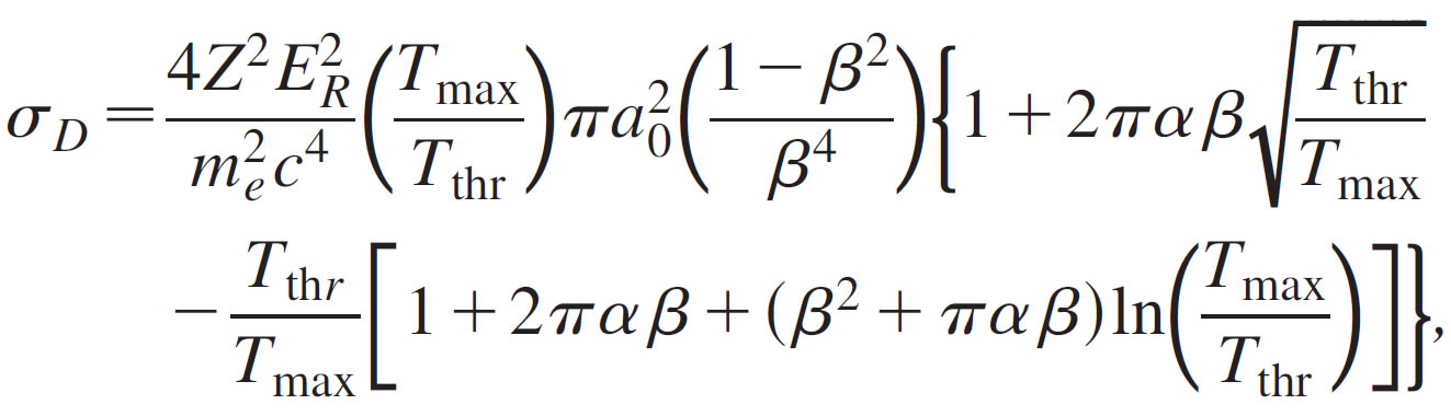
with Z: atomic number of the target atoms, ER = 13.6 eV Rydberg energy, a0 = 5.3 x 10⁻¹¹ m Bohr radius of the hydrogen atom, β = ve/c electron velocity ve divided by the speed of light c, me mass of the electron, α ≈ Z/137, Tmax maximum transferred energy in the collision event, and Tthr = 22 eV threshold energy for atomic displacement [6, 32, 33].
Without modifications, this equation is suitable to evaluate the total "knock-on" cross section for an atom at rest with a given ejection threshold energy. The curve in Fig. 5 ("static lattice") shows a rather sharp onset of radiation damage with increasing acceleration voltage: the scattering cross section is 0 up to a well-defined limit value (108 kV), and rises to values beyond the range of measured values only some kV above this limit. The change of the displacement threshold in the equation above shifts the curve sideways, but does not change the sharp onset. Hence, this equation is independent of the threshopd energy, in clear contradiction to the observations showing a smooth onset of the damage cross section between 80 and 100 kV.
Now the scientists made a modification to the above equation that considered that an atom oscillating parallel to the electron beam can obtain a higher transferred energy Tmax than if it were static. When the struck atom’s vibrations on its own displacement are taken into account the experimental data can be explained. This effect was previously discussed, e. g. [20] and the new measurements provide precise experimental evidence of this intriguing effect. They approximated the vibrations of the atoms within the framework of the Debey model and use the Debey temperature for 12C - graphene ΘD = 1287 K [34]. The temperature for 13C graphene is given by ΘD13=(12/13 Θ 12/D)0.5, since Θ depends on the sound velocity. The calculation of the atomic velocities in the beam direction and the electron energy yields the maximum transferred energy Tmax(ν,E). This gives them the distribution of the sputtering cross section numerically (see Supplemental Material). In other words, they still used the scattering cross-section according to the above equation, but took into account that the atoms are not at rest.
"The threshold energy was derived from first principles calculations without any modification. With these values, the smooth onset of the knock-on damage can be reproduced very well between 80 and 100 kV. We showed for the first time that the threshold energy can be used without adjustments to reproduce the experimental data," said Meyer. "The threshold energy was not calculated incorrectly in previous studies, but the lattice vibrations were not taken into account."
Resource: Meyer, J. C., Eder, F., Kurasch, S., Skakalova, V., Kotakoski, J., Park, H. J., Roth, S., Chuvilin, A., Eyhusen, S., Benner, G., Krasheninnikov, A. V., and Kaiser, U. A. (2012). Accurate measurement of electron beam induced displacement cross sections for single-layer graphene. Physical review letters, 108: 196102, doi: 10.1103/PhysRevLett.108.196102, [PDF], see also the supporting information PDF, supporting information Video 1, Video 2, Video 3, Video 4 and Video 5.
Meyer, J. C., Kurasch, S., Park, H. J., Skakalova, V., Künzel, D., Groß, A., Chuvilin, A. Algara-Siller, G., Roth, S., Iwasaki, T., Starke, U., Smet, J., & Kaiser, U. (2011). Experimental analysis of charge redistribution due to chemical bonding by high-resolution transmission electron microscopy. Nature materials, 10: 209-215, doi: 10.1038/nmat2941
Meyer, J. C., Kisielowski, C., Erni, R., Rossell, M. D., Crommie, M. F., & Zettl, A. (2008). Direct imaging of lattice atoms and topological defects in graphene membranes. Nano letters, 8: 3582-3586, doi: 10.1021/nl801386m
Banhart, F. (1999). Irradiation effects in carbon nanostructures. Reports on Progress in Physics, 62: 1181, doi: 10.1088/0034-4885/62/8/201
Lucas, M. W., & Mitchell, E. W. J. (1964). The threshold curve for the displacement of atoms in graphite: Experiments on the resistivity changes produced in single crystals by fast electron irradiation at 15 K. Carbon, 1: 345-352, doi: 10.1016/0008-6223(64)90290-8
Smith, B. W., & Luzzi, D. E. (2001). Electron irradiation effects in single wall carbon nanotubes. Journal of Applied Physics, 90: 3509-3515, doi: 10.1063/1.1383020
Krasheninnikov, A. V., Banhart, F., Li, J. X., Foster, A. S., & Nieminen, R. M. (2005). Stability of carbon nanotubes under electron irradiation: role of tube diameter and chirality. Physical Review B, 72: 125428, doi: 10.1103/PhysRevB.72.125428
Egerton, R. F., Li, P., & Malac, M. (2004). Radiation damage in the TEM and SEM. Micron, 35: 399-409, doi: 10.1016/j.micron.2004.02.003
Iijima, S. (1991). Helical microtubules of graphitic carbon. Nature, 354: 56-58, doi: 10.1038/354056a0
Iijima, S., & Ichihashi, T. (1993). Single-shell carbon nanotubes of 1-nm diameter. Nature, 363: 603–605, doi: 10.1038/363603a0
Kroto, H. W., Heath, J. R., O'Brien, S. C., Curl, R. F., & Smalley, R. E. (1985). C 60: buckminsterfullerene. Nature, 318: 162-163, doi: 10.1038/318162a0
Novoselov, K. S., Geim, A. K., Morozov, S. V., Jiang, D., Zhang, Y., Dubonos, S. V., Grivorieva, I. V. & Firsov, A. A. (2004). Electric field effect in atomically thin carbon films. Science, 306: 666-669, doi: 10.1126/science.1102896
Geim, A. K., & Novoselov, K. S. (2007). The rise of graphene. Nature materials, 6: 183-191, doi: 10.1038/nmat1849
Pacile, D., Meyer, J. C., Girit, C. O., & Zettl, A. (2008). The two-dimensional phase of boron nitride: few-atomic-layer sheets and suspended membranes. Applied Physics Letters, 92: 133107, doi: 10.1063/1.2903702
Haider, M., Uhlemann, S., Schwan, E., Rose, H., Kabius, B., & Urban, K. (1998). Electron microscopy image enhanced. Nature, 392: 768-769, doi: 10.1038/33823
Batson, P. E., Dellby, N., & Krivanek, O. L. (2002). Sub-angstrom resolution using aberration corrected electron optics. Nature, 418: 617-620, doi: 10.1038/nature00972
Suenaga, K., Sato, Y., Liu, Z., Kataura, H., Okazaki, T., Kimoto, K., Sawada, H., Sasaki, T., Omoto, K., Tomita, T., Kaneyama, T., & Kondo, Y. (2009). Visualizing and identifying single atoms using electron energy-loss spectroscopy with low accelerating voltage. Nature Chemistry, 1: 415-418, doi: 10.1038/nchem.282
Muller, D. A., Kourkoutis, L. F., Murfitt, M., Song, J. H., Hwang, H. Y., Silcox, J., Dellby, N. & Krivanek, O. L. (2008). Atomic-scale chemical imaging of composition and bonding by aberration-corrected microscopy. Science, 319: 1073-1076, doi: 10.1126/science.1148820
Bar Sadan, M., Houben, L., Wolf, S. G., Enyashin, A., Seifert, G., Tenne, R., & Urban, K. (2008). Toward atomic-scale bright-field electron tomography for the study of fullerene-like nanostructures. Nano letters, 8: 891-896, doi: 10.1021/nl073149i
Egerton, R. F., McLeod, R., Wang, F., & Malac, M. (2010). Basic questions related to electron-induced sputtering in the TEM. Ultramicroscopy, 110: 991-997, doi: 10.1016/j.ultramic.2009.11.003
Zag, W., & Urban, K. (1983). Temperature dependence of the threshold energy for atom displacement in irradiated molybdenum. Physica Status Solidi A, 76: 285-295, doi: 10.1002/pssa.2210760133
Kotakoski, J., Krasheninnikov, A. V., Kaiser, U., & Meyer, J. C. (2011). From point defects in graphene to two-dimensional amorphous carbon. Physical Review Letters, 106: 105505, doi: 10.1103/PhysRevLett.106.105505
Meyer, J. C., Girit, C. O., Crommie, M. F., & Zettl, A. (2008). Imaging and dynamics of light atoms and molecules on graphene. Nature, 454: 319-322, doi: 10.1038/nature07094
Park, H. J., Meyer, J., Roth, S., & Skákalová, V. (2010). Growth and properties of few-layer graphene prepared by chemical vapor deposition. Carbon, 48: 1088-1094, doi: 10.1016/j.carbon.2009.11.030
Kaiser, U., Biskupek, J., Meyer, J. C., Leschner, J., Lechner, L., Rose, H., Stöger-Pollach, M., Khlobystov, A. N., Hartel, P., Müller, H., Haider, M., Eyhusen, M., & Kaiser, U. (2011). Transmission electron microscopy at 20kV for imaging and spectroscopy. Ultramicroscopy, 111: 1239-1246, doi: 10.1016/j.ultramic.2011.03.012
Girit, Ç. Ö., Meyer, J. C., Erni, R., Rossell, M. D., Kisielowski, C., Yang, L., Park, C.-H., Crommie, M. F., Cohen, M. L., Louie, S. G., & Zettl, A. (2009). Graphene at the edge: stability and dynamics. Science, 323: 1705-1708, doi: 10.1126/science.1166999
Kotakoski, J., Santos-Cottin, D., & Krasheninnikov, A. V. (2011). Stability of graphene edges under electron beam: equilibrium energetics versus dynamic effects. ACS Nano, 6: 671-676, doi: 10.1021/nn204148h
Mølhave, K., Gudnason, S. B., Pedersen, A. T., Clausen, C. H., Horsewell, A., & Bøggild, P. (2007). Electron irradiation-induced destruction of carbon nanotubes in electron microscopes. Ultramicroscopy, 108: 52-57, doi: 10.1016/j.ultramic.2007.03.001
Barreiro, A., Börrnert, F., Avdoshenko, S. M., Rellinghaus, B., Cuniberti, G., Rümmeli, M. H., & Vandersypen, L. M. (2013). Understanding the catalyst-free transformation of amorphous carbon into graphene by current-induced annealing. Scientific reports, 3: 1115, doi: 10.1038/srep01115
Kotakoski, J., Meyer, J. C., Kurasch, S., Santos-Cottin, D., Kaiser, U., & Krasheninnikov, A. V. (2011). Stone-Wales-type transformations in carbon nanostructures driven by electron irradiation. Physical Review B, 83: 245420, doi: 10.1103/PhysRevB.83.245420
Mott, N. F. (1929). The scattering of fast electrons by atomic nuclei. Proceedings of the Royal Society of London A, 124: 425-442, doi: 10.1098/rspa.1929.0127
McKinley Jr, W. A., & Feshbach, H. (1948). The coulomb scattering of relativistic electrons by nuclei. Physical Review, 74: 1759, doi: 10.1103/PhysRev.74.1759
Zobelli, A., Gloter, A., Ewels, C. P., Seifert, G., & Colliex, C. (2007). Electron knock-on cross section of carbon and boron nitride nanotubes. Physical Review B, 75: 245402, doi: 10.1103/PhysRevB.75.245402
Kotakoski, J., Jin, C. H., Lehtinen, O., Suenaga, K., & Krasheninnikov, A. V. (2010). Electron knock-on damage in hexagonal boron nitride monolayers. Physical Review B, 82: 113404, doi: 10.1103/PhysRevB.82.113404
Tewary, V. K., & Yang, B. (2009). Singular behavior of the Debye-Waller factor of graphene. Physical Review B, 79: 125416, doi: 10.1103/PhysRevB.79.125416