Partnership
Ulm University has defined their future oriented research areas, which include nano- and biomaterials as well as functional ultra-high resolution imaging. The claim of EMMS (group of electron microscopy of materials science) in the Central Facility for Electron Microscopy is to use and develop techniques that allow structural analysis of these challenging materials at the level of state of the art electron microscopy. As with any experimental technique, this implies state of the art instrumentation. We were lucky to receive one of the first commercially delivered aberration corrected electron microscopes in 2005, the FEI Titan 80-300. Very soon we discovered the great advantages to work on electron beam sensitive materials at 80 kV. Moreover, we discovered the limitations at this voltage, wherefrom our SALVE project received its inspiration.
The SALVE collaboration is therefore focused on exploring still largely undiscovered territory in electron microscopy: high-resolution imaging and spectroscopy at low voltages from 20 kV to 80 kV. Imaging beam-sensitive objects in a transmission electron microscope is a very challenging experiment, because the same electrons that are responsible for the astonishing imaging power of modern TEMs also modify the specimen that they probe: the incident electron beam interacts with the atoms and bonds within the probed material, eventually causing irreversible damage. It is known, however, that compared to typical accelerating voltages of 80 kV or more, this beam-sample interaction takes on an entirely different character at even lower acceleration voltages. At the same time, the elastic (i.e. non-damaging) interaction of the electrons with the material increases, promising potentially more structural information per incident electron due to the enhancement of contrast. Main tasks within the SALVE project are exploring the consequences of a reduction in electron acceleration voltage and developing strategies for optimizing imaging under these conditions.
In SALVE I-II industry partners of Ulm University were Carl Zeiss Microscopy and CEOS GmbH. We have completed a feasibility study for optimizing a CS aberration corrected TEM for operation at low voltages down to 20 kV in SALVE I [1]. In the second phase a CS/CC corrector has been built and tested [2]. Based on improved dose-dependent image simulation validated by results achieved with this new corrector we are now able to calculate the dose-dependent image contrast for low voltage operation using image spread and focus spread values.
Application related experiments involve not only the determination of the crystallographic and electronic structure, but also in-situ observation in real time. This requires adequate novel sample holder technologies. In SALVE II, we determined the technical specifications that must be met for a low‐noise sample carrier to enable in-situ operating condition using the joint co-operation of the EMMS physicists and micro- and nano-structure engineers at Ulm University.
Together with researchers from different fields (the SALVE science team) a wide-spread variety of materials are investigated in SALVE I-III: carbon nanotubes filled with metals or molecules, semiconductor and oxide membranes, catalysts and porous materials, battery materials containing sulfur, lithium, magnesium, or fluorides, as well as functionalized graphene, other two-dimensional materials, and the adsorbate-2D material interaction. The results have been underpinned by theory (DFT-simulations).
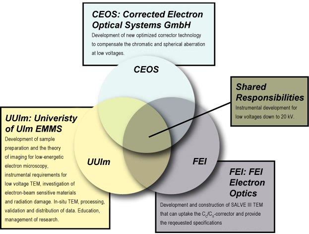
SALVE III project partners of Ulm University are FEI Company and CEOS GmbH. From the first two project phases, Ulm University and CEOS GmbH bring in valuable results about TEM at very low voltages consisting of information about which sample to investigate (this however is an ongoing process with biomolecules and anorganic-organic interfaces in the centre), sample preparation and the CS/CC-corrector design. FEI Company has already addressed the low-voltage TEM business and brings in valuable information about different hardware components for operation at acceleration voltages well below 80 kV. We are very glad that the FEI Company once again invested in aberration-corrected high-resolution TEM after the so successful first aberration-corrected instruments as well as the TEAM and PICO projects in the past. The first resolution improvement by a factor of 2 from 0.24 nm to 0.13 nm was realized for a 200 kV FEI-CS-corrected TEM in 1998 [3] and the second resolution improvement to 0.055 nm was realized for a CS/CC-corrected 80-300 kV S/TEM operated at 200 kV in 2010 [4]. In tradition to these pioneer projects, we investigate with the actual SALVE project together with FEI and CEOS the next generation of aberration corrected high resolution TEMs with very low voltages down to 20 kV to resolve soft materials and we are best prepared to address this task of SALVE operation with our long-year experience in experiments, calculation, and sample preparation.
- Kaiser, U., Biskupek, J., Meyer, J. C., Leschner, J., Lechner, L., Rose, H., Stöger-Pollach, M., Khlobystov, A. N., Hartel, P., Müller, H., Haider, M., Eyhusen, S., & Benner, G. (2011). Transmission electron microscopy at 20kV for imaging and spectroscopy. Ultramicroscopy, 111: 1239-1246, doi: 10.1016/j.ultramic.2011.03.012
- Haider, M., Uhlemann, S., Hartel, P., & Müller, H. (2014). Towards High Resolution in TEM and STEM: What are the Limitations and Achievements. Microscopy and Microanalysis, 20: 378-379, doi: 10.1017/S1431927614003614
- Haider M., H. Rose, S. Uhlemann, E. Schwan, B. Kabius, K. Urban, 1998: A spherical-aberration-corrected 200 kV transmission electron microscope. Ultramicroscopy, 75:53-60, doi: 10.1016/S0304-3991(98)00048-5
- Haider, M., Hartel, P., Müller, H., Uhlemann, S., & Zach, J. (2010). Information transfer in a TEM corrected for spherical and chromatic aberration. Microscopy and Microanalysis, 16: 393-408, doi: 10.1017/S1431927610013498
About the University of Ulm
The University of Ulm is situated in the east of Baden-Württemberg at the river Danube. The research, studying, and teaching activities concentrate on medicine, economics, natural science, engineering and material science. About 10,000 students are currently enlisted at the University of Ulm. The electron microscopy group headed by Ute Kaiser is well-known for the research in the field of low-voltage TEM and its application to novel beam sensitive materials such as low-dimensional objects. The group was one of the first adopters and users of aberration-corrected TEM technology with the FEI-TITAN already in 2005. In 2008 Ute Kaiser started to establish the SALVE project with the aim of developing the prerequisites for transmission electron microscopy capable to reach atomic resolution at 20 kV. More information can be found at: www.uni-ulm.de.
About FEI Company
FEI Company (Nasdaq: FEIC) designs, manufactures and supports a broad range of high-performance microscopy workflow solutions that provide images and answers at the micro-, nano- and picometer scales. Its innovation and leadership enable customers in industry and science to increase productivity and make breakthrough discoveries. Headquartered in Hillsboro, Ore., USA, FEI has over 2,600 employees and sales and service operations in more than 50 countries around the world. More information can be found at: www.fei.com.
About CEOS GmbH
CEOS GmbH is a privately owned SME which concentrates on the developments and research of advanced charged particle optical components like aberration correctors for high resolution TEMs and STEMs as well as SEMs. Most of these components are produced by CEOS and after factory alignment and proper testing shipped as OEM products to the EM manufacturers. CEOS is located in Heidelberg, Germany and has more than 40 employees. More information can be found at: www.ceos-gmbh.de.
The project partners collaborate openly with the international microscopy community and will promote the technology transfer of advanced low-voltage electron microscopy. Moreover knowledge and experience obtained from the SALVE III project will be passed on to the next generation of microscopists and other researchers from universities, institutes and industry.